This thread has been locked.

If you have a related question, please click the "Ask a related question" button in the top right corner. The newly created question will be automatically linked to this question.

TPS65132: TPS65132W (80mA) -vs- TPS65132S (150mA)

Part Number: TPS65132


Tool/software:

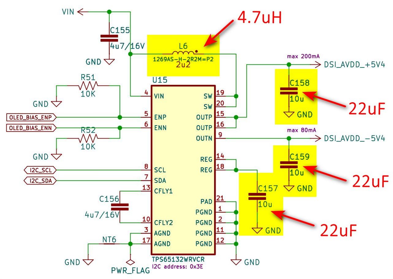
We are using TPS65132W in the 80mA mode.


But, 80mA is on the edge for our application, and we'd like to design a bit of a reserve.

  • Any recommendations / insights on how to go about it?

Our first thought is to simply beef up the capacitors around it: C155, C156, C157, C158, C159, such as by doubling them.

We have also tried using the "S" part, but found it difficult to route. Moreover, it is not clear how a smaller BGA can provide more current than a part that comes with a PowerPAD.


It would greatly help us to understand how the "S" variant goes about its stated high power ability, and whether we can apply some of its recipe to the "W" that we already have on the board, and are reluctant to change. The "S" SYNC input seems to be critical to that. We have FPGA connected to both ENP and ENN inputs and, if needed, can apply complex pattern on them.

  • Hi ,

    May I check what's the end equipment for this case? and what's the max loading here?

    The S version has some design changes to support larger loading, like additional headroom and larger OCP value...

    BRs,

    Young

  • The display in question is dual 0.49" FHD micro-OLED.

    BTW, while looking around, we ran into a similar discussion: e2e.ti.com/.../tps65132-tps65132wrvcr-output-voltage-drop. The option of changing the inductor from 2.2uH to 4.7uH is touched upon there, as well as checking inductor saturation current. Our inductor is 1269AS-H-2R2M=P2, which saturates at 2.2A.

    We are not concerned about VPOS output, as it comes with 200mA output capacity. Our typical VNEG load is 2 x 30mA. But, the OLED vendor says that the max into their display can be as much as 2 x 100mA. They did not explain how such wide variations are possible. We are also pushing on them to learn about the duration of that high loading condition, and whether it can qualify as a transient glitch.

  • Hi,

    Like I said above, S version imply with much larger headroom and larger OCP to support larger loading. Otherwise, it would be limited by the headroom and OCP, and then output voltage drops.

    based on your application, could you help share the specs for confirmation? Or pls send the spec to young-zhao@ti.com by mail.

    BRs,

    Young

  • It should be related with the critical picture and make the loading variation so much large. I would suggest S version if the POS/NEG loading may up to 200mA. Let us know if any concern regarding this part.

  • Our layout designer reported difficulties routing the "S" part BGA. As the project schedule was under fire at that time, and solely in the interest of saving time, we've switched to the "W" part. We must admit that the "W" also looked more robust thanks to its large "PowerPad".

    While we are now looking to switch back to the "S" part in the next board spin, until it comes, we wonder if there is anything we can do within the constraints of the existing PCB to boost the VNEG/AVEE capability beyond 80mA?

    - We have I2C access and can adjust all register settings, possibly raising the OCP limit. 
    - We can use larger capacitors around the TI part
    - We can increase the inductor from 2.2uH to 4.7uH if you believe that would help

    This is to solicit your commentary on these stopgap measures, as well as additional thoughts on enabling higher AVEE currents in the existing PCB framework.

    ----
    Additional references:
    e2e.ti.com/.../4004894
    e2e.ti.com/.../3411480

  • Hi

    I did check the function with internal team. 

    1) LDO output (POS) OCP is same for S and other version, only CPN OCP and headroom voltage are different. 

    2) S version die is different, even W version can access the register , it still cannot trigger the 150mA loading as no SYNC pin function.

    So I would suggest to add more output caps and REG caps and 4.7uH to store more power to sustain the voltage stable during larger loading transient with W version. 

    BRs,

    Young

  • Thank you, that's very good info!

    Would you please recommend the output cap values to use? Do you see benefit in also increasing the CPN "flying" cap? Perhaps even input capacitor, and to what values?

    Any more detail you can share on that special "register" and SYNC pin mechanism that allows the circuitry to deliver more juice. Is it fair to say that, given that the "S" version does not have a large PowerPAD, the "W" version does not really need that cooling function, which is essentially redundant on the "W"?!

  • Hi 

    For output POS/NEG, pls enlarge them to 2x10uF and reserve one more place if more caps needed. For REG caps, pls reserve 1 caps here. No need to change the clfy cap.

    And sorry that I cannot share more details regarding the internal register information. 

    BRs,

    Young

  • Given our objective to improve the situation within framework of the existing PCB, can we summarize your recommendation as follows:

    - increase C157, C158, C159 from its current 10uF to 22uF

    - increase L6 from its current 2.2uH to 4.7uH


    Please confirm. Could you please also quantify the expected effect of this upgrade.

    - Would it be possible to solidify this answer by providing the results of before and after simulations?!


  • Hi,

    Our expert will update you soon

  • ... while at it, could you please have him/her also comment on the options for boosting the VNEG current capability of the "S" part from its specified 150mA to, if possible, something like 200mA short-term surge.

       - Would the same scheme, where the L and Cs are doubled, also work there?

    How much extra juice would it provide? Is there a yet better approach for that case, where we also enjoy the freedom to change the schematic and layout, not only the BOM?!

    That's in prep for our Rev.B board, which will replace the "W" with "S" part, and where we also look for ways to set the "S" for an above-and-beyond power delivery performance...

  • Hi,

    Adding L and cap will reduce ripple and increase stability. It is no use to enlarge the IC long term output current capability.

    But 200mA short-term surge is feasible as long as you increase the output cap. I think 22uF is enough but it is better to keep one more cap position which is unsoldered.

    Thanks,

    Colin

  • Are you thinking of a 10uF for that unsoldered backup position? Or another 22uF?

  • Yes, another 22uF is good.

    Thanks,

    Colin