Other Parts Discussed in Thread: IWR1843BOOST
Tool/software:
Dear Team,
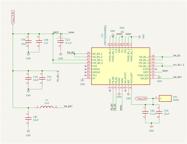
I have designed a schematic for the LP87702-Q1 buck converter. I plan to test it in standalone operation without any digital input/ouput other than a 3.3V Vin.
My target outputs are:
-
1.8V from SW_B0
-
1.24V from SW_B1
-
5V from VOUT_BST
I have followed the schematic checklist (https://www.ti.com/lit/zip/snvr494).
For the pin configuration:
-
CLK, SDA, SCL, EN1 are tied to GND
-
GPO0, PG0, PG1, VMON1, VMON2 are left unconnected
For this design, and the schematics are attached below for your reference.


Could you please confirm if there is anything I might have missed?
Also, can this schematic operate under the conditions described above?
Thank you in advance for your support.


