Tool/software:
Summary of LM5017MRX/NOPB issues:
Application:
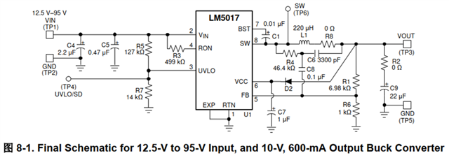
Household storage drive auxiliary power source, input voltage 21-46.5V, one winding on the primary side outputs 10.5V load 300mA, two windings on the secondary side each output 10.5V load 40mA.
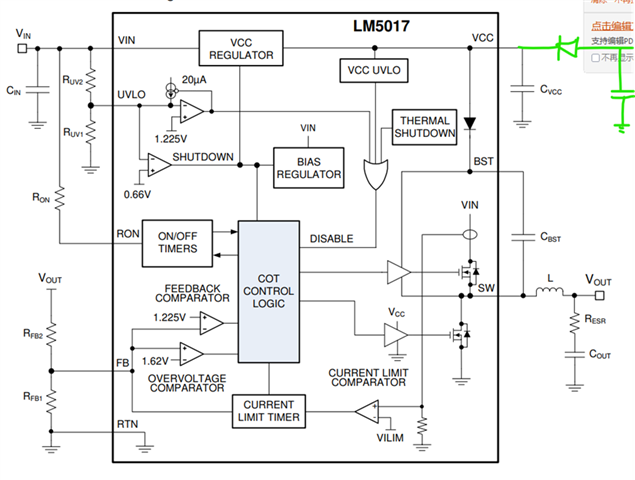
- LM5017 Bootstrap capacitor:
In the application circuit, the specification of the BST capacitor is 0.01uF. Based on our previous application experience, we have adjusted the capacitor to 100nF.。
Question
- What considerations are behind setting 10nF? Does adjusting the capacitor to 100nF have any impact on the internal circuit
- Could you provide the inrush current capacity of the internal BST diode at 100℃
- Is there a current-limiting resistor inside the BST capacitor charging circuit? If so, what is it?

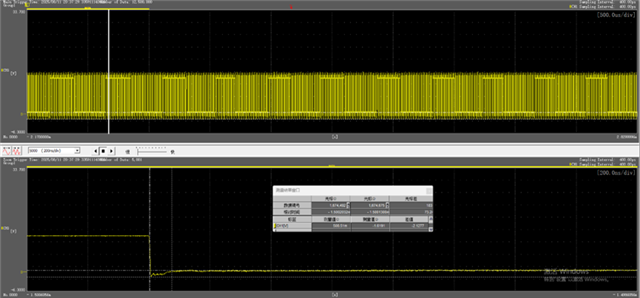
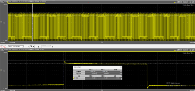
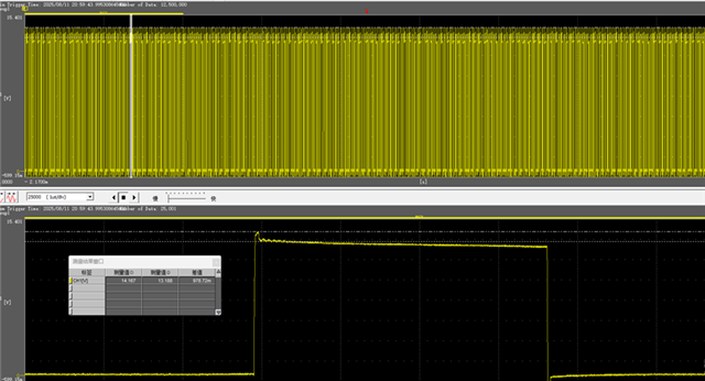
When the BST voltage of the self-lifting capacitor 100nF was established to 7.6V upon startup, there was no impulse. At the moment of wave generation, there was an impulse current of approximately 38mA (impulse current during wave generation upon startup), as shown in the following figure.
The BST voltage follows the external Vcc voltage. When starting up and generating waves, when the second wave begins and the external voltage exceeds the internal LDO output of 7.6V, an inrush current will be generated, which will impact the internal BST.
2.Voltage stress of SW-RTN
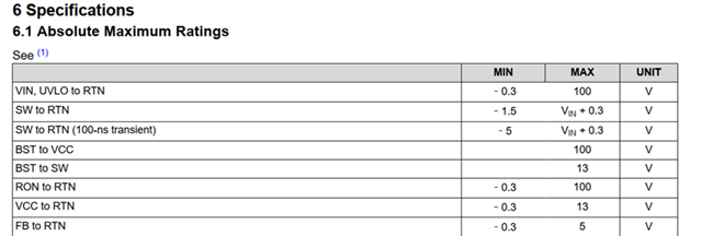
Question
- The stress parameter in the SW-RTN specification sheet is Vin+0.3V. What considerations are behind 0.3V? Is it out of concern that the upper body diode may be damaged by a large current in a short time, or are there other components inside that cannot withstand the high voltage? Is Vin Max=100V or the actual input voltage?
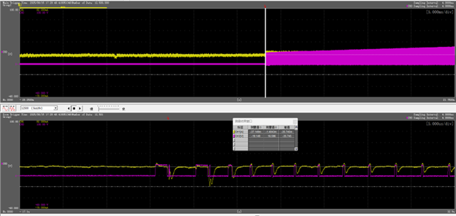
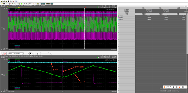
- For SW-RTN, we detected a Spike of Vin+1V (Vin=13.2V) under light load. By increasing the Vin voltage, the Spike rose to Vin+2V (Vin= 25V). Help assess whether there is any risk in this.
The conduction voltage drop of the upper body diode will clamp the SW-RTN to Vin+0.3V. Therefore, the specification sheet provides a theoretical clamping value and does not necessarily have to be lower than this value.。
3.SW-VIN voltage stress
Question
Does the SW-Vin specification (upper MOS stress) need to be reviewed in reference to SW-RTN?
We test ourselves to have a negative Spike of -2.1V@73ns and a positive Spike of +1.4V@87ns. Help assess whether there is any risk in this positive or negative specification of SW-Vin and how it is considered。