This thread has been locked.

If you have a related question, please click the "Ask a related question" button in the top right corner. The newly created question will be automatically linked to this question.

LM5109A: Driving a complementary (NMOS/PMOS) power FET pair

Part Number: LM5109A
Other Parts Discussed in Thread: UCC21550, UCC21551, UCC21231

Dear TI,

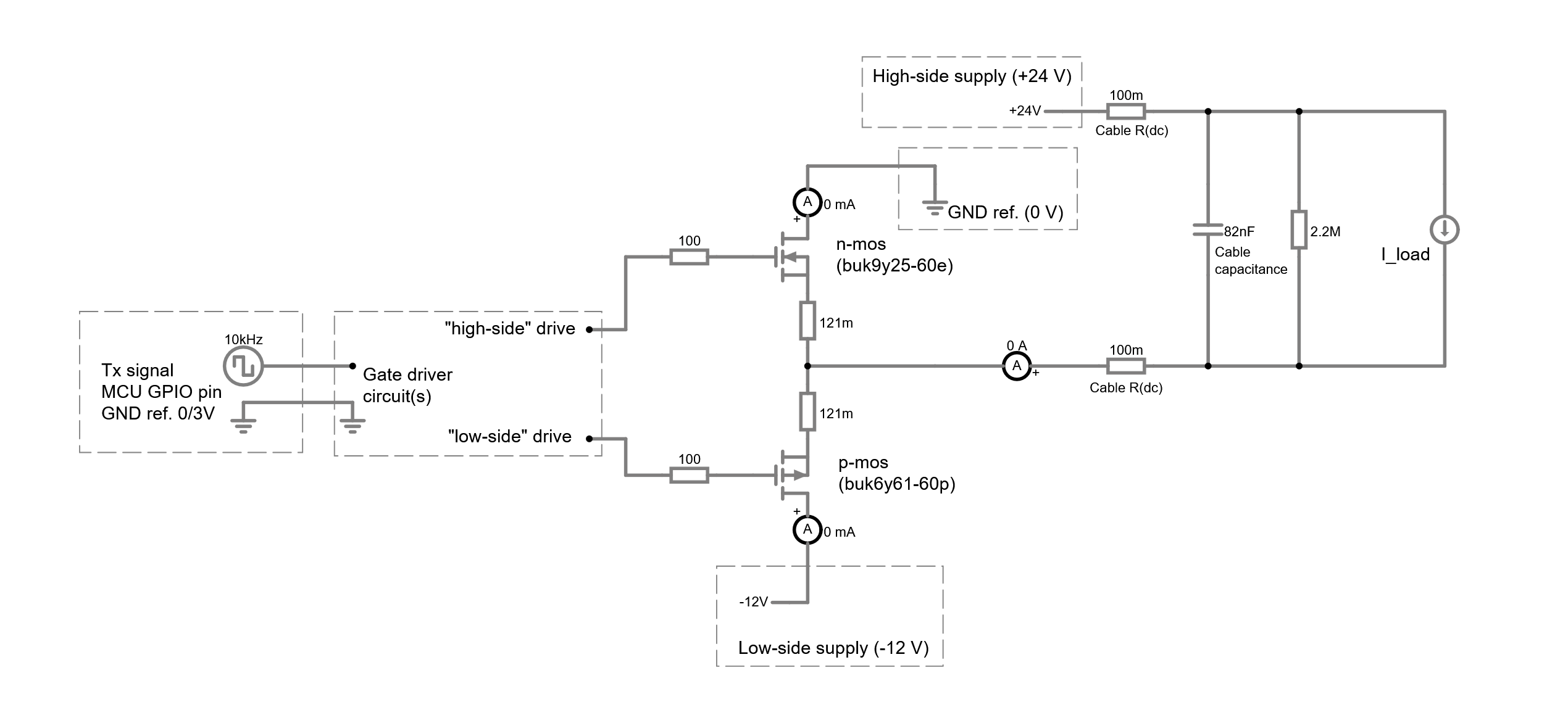
I would like to ask whether the LM5109A would be suitable for use in the following communication application. 

The goal would be to steer the load current (I_load) either into ground (0 V) or low side supply (-12 V) based on a 0/3V digital signal coming from a microcontroller. This should then switch the lower side of the communication cable between -12 V and 0 V. The upper side of the cable stays fixed at +24 V potential.

The difficulty I'm facing is designing the drive circuit for the N-channel and P-channel MOSFET switches. The P-channel device has -12V reference, so (I think) it cannot be controlled directly via microcontroller output pin.

I would be grateful for any thoughts, advice or gate driver product recommendations. Thank you!


fet_drive.png

  • Hi Arttu,

    We do not recommend using any non-isolated half bridge gate driver in this way. This is not the intended use for this driver for many reasons. First, when in the undervoltage lockout state, both of the gates will be held low, thus the PMOS always be ON the lower side of the cable will always be pulled to -12V. 

    The primary problem with this setup is that the MCU and the non-isolated driver need to have the same ground reference on the low side.

    If this is a requirement, I recommend using an isolated gate driver. 

    I am going to move this thread to our isolated gate driver team, they will be able to best assist you with the selection of an isolated gate driver for this application. 

    Best,

    Amy

  • Thank you Amy for your information and good point on undervoltage lockout.

    Sure, please go ahead and move this thread into a suitable sub-forum.

  • Hi Arttu,

    Based on the initial schematic you have sent, UCC21550/UCC21551 would be the isolated gate driver that should work for your application. This is a dual-channel gate driver, so it allows for two outputs similar to the system you have configured in your schematic. If a smaller package size is needed, then UCC21231 would be a great option as well, as it is very similar to UCC21550/UCC21551. I would start by looking into these first, and if you have any other questions, please feel free to reach out!

    Best regards,

    Will

  • Hello Will,

    thank you for suggesting UCC21550 and UCC21231. I will consider them in my current design.

    Looking at UCC21550 datasheet, its intended purpose is to drive two N-channel transistors as shown in "Figure 8-1. Typical Application Schematic". Low-side FET Source is tied to VSSB/isolated ground, which is different from my use case in this application. In such Fig. 8-1 configuration the IC provides shoot-through protection. Would this feature be lost when driving a P-/N-channel MOSFET pair?

    This got me wondering if I could use the UCC21550 with two N-channel FETs? The lower side, or wire, of the cable would be tied to ground and its upper side/wire would be switched between 36V and 24V as shown in the sketch below.

    Which kind of charge pump circuit would you recommend to be used for driving the upper (36V) N-channel FET? The design is complicated by the fact that the circuit might spend majority of its time with the upper N-FET fully enhanced and providing 36V to the load(s), e.g. the duty cycle of the upper transistor switch could certainly be close to 100 %.

  • Hi Arttu,

    In terms of a charge pump circuit, I would recommend to read into these TI technical articles about charge pump circuits which have a lot of great information on the different topologies you can use in your system: [Link 1] [Link 2] [Link 3] [Link 4]

    Best regards,

    Will