Other Parts Discussed in Thread: LM5013
Hi,
I decided to go with LM5013-Q1 and initially planned to follow the LM5013-Q1 EVM schematic. However, I’ve encountered some inconsistencies that make it difficult to move forward confidently:
-
The BOM and schematic for the EVM do not match in capacitor values (specifically for C8 and C9).
-
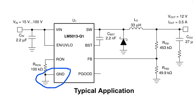
The SNVR514 — LM5013-Q1 Design Calculator shows a schematic where the GND pin is not connected to ground, which seems incorrect.
I’m not trying to flag errors, but I’m building a large prototype board, and I want to avoid small yet costly design mistakes.
Could you please point me to the most up-to-date and internally consistent reference (datasheet, EVM design, or validated schematic) that I can rely on for the LM5013 or LM5013-Q1?
Your clarification would help restore confidence that I’m aligning with the correct TI design guidance.


Best Regards,
Mohammed