LM5122-Q1: LM5122 becomes unstable above 50% duty cycle.

Part Number: LM5122-Q1
Other Parts Discussed in Thread: LM5122, LM5085

I implemented a solution using LM5122 to boost Votlage from 12V to 50V. The solution proposed by WeBench was implemented:

webench.ti.com/.../14

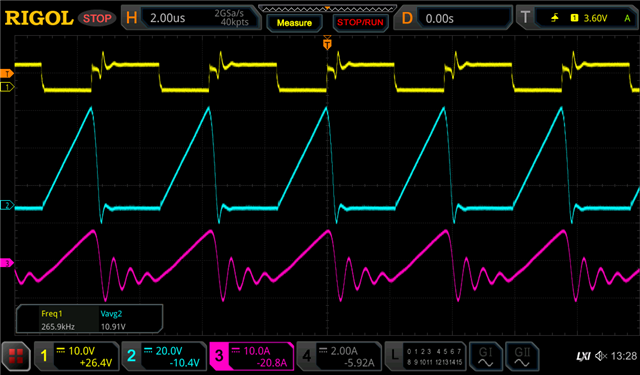
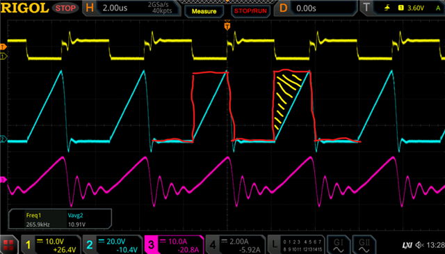
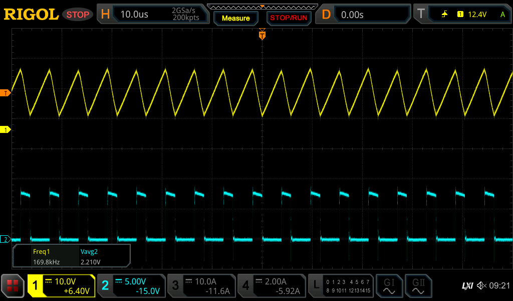
This solution is unstable when boosting to 50V. The data sheet suggests that it might be a problem when the duty cycle is >50% and that the Slope control should be used.

I reduced the boost Voltage and found that it was stable up to around 50% duty which gave only around 20V.

I found some problems with the formulae for calculating the Slope reLM5122 WeBench Circuit.jpgLM5122.pngsistor. Section 7.3.4 shows a formula for Rslope that includes a constant 'K' and the formula for 'K' includes the value for Rslope, so there's a circular argument and neither can be solved.

After experimenting with Slope resistor values I made some improvements and have increased stability for Voltages up to 30V.

Without a robust method for properly calculating Rslope it will take a long time to resolve.

Also, should the loop compensation components change when the Slope control changes?

  • Hello Lee,

    Thanks for using the e2e forum.
    Slope compensation and feedback loop compensation are not dependent of each other, but both are mandatory for a stable system.
    Slope compensation avoid subharmonic oscillation and duty cycle jittering, while loop compensation affects general regulation stability.

    I would double check the K factor value and the loop compensation with our quickstart calculator tool.
    This tool takes more entries than the webench tool, so the results are generally more accurate.

    https://www.ti.com/tool/download/LM5122-BOOST-CALC

    You can also fill in the calculator and sent it back to me, so I can double check all entries for potential root cause of the instability.

    Best regards,
    Niklas

  • Thank you Niklas,

    Attached is the calculator tool with my values applied. My solution has a large output capacitance (3000uF) so that isn't a typo, it's a design requirement.

    In order to get the phase margin around 60° I had to select compensation values that are quite diffeent to those suggested, are these correct or did I misunderstand something.

    Any feedback you can give would be appreciated.

    Thanks,LM5122_Quickstart_Calculator_V1_1_0 - Mod.xlsx

  • Also, do you have a similar calculation tool for the LM5085 device?

    Thanks.

  • Hi Lee,

    Thanks for the calculator entries.
    You used the tool correctly to get a compensation recommendation.
    When a large output capacitance of 3mF is used, a the regulation system and the loop compensation becomes very slow. This is why the calculated compensation values become rather large. The field for the Cout ESR (line 59) also becomes more relevant for the compensation calculation.
    Essentially, the compensation calculation is not wrong, but the system becomes so slow by itself, that a high crossover frequency is not possible anyway. As long as the compensation is not completely unstable, you might no see notable differences in the transient response if smaller values are used.

    You selected a slope compensation resistor of 27kOhm. This is smaller than the recommended value of both quickstart calculator and webench.
    Did you achieve better results with this resistance?
    If you see instability at higher duty cycles, this might be the most likely culprit.

    The LM5085 is from another product line, so I am no expert for this device, but I found this calculator tool on the according product page:
    https://www.ti.com/lit/zip/snvu075

    Best regards,
    Niklas

  • Thanks Niklas,

    I chose a value for the slope comp resistor that was between Min and Calc slope resistor values, should I get closer the calc value?

    The circuit is working much better now, there is no apparent instability, so the calc tool seems to have worked ok.However, the main FET switch is getting too hot. I didn't use the FET that WeBench proposed, could the choice of FET be the cause of the overheating? The part I'm using is BUK765R0-100E

    https://assets.nexperia.com/documents/data-sheet/BUK765R0-100E.pdf

    The red trace shows the FET current, could the oscillation of current in the FET cause the heating? Do you have any insight on this please?

  • Hi Lee,

    I am glad to hear that the value changes based on the calculator tool helped to improve the design.
    You can go even closer to the calc value to check for further improvements.

    Do you use gate resistors at the MOSFETs? The slower the MOSFETs switch, the higher the potential losses and the higher the temperature.
    I also assume you did some blue-wiring to connect the in-line current probes to measure the inductor and MOSFET currents.
    Layout can also have a large effect on losses and thermal behavior, so this modification may add to the overtemperature problem.

    Based on the MOSFET datasheet, I do not directly see any problems with the part itself.

    Best regards,
    Niklas

  • Hi Niklas,

    Thanks for the contiuned help.

    No, I have no resistor in the gate, but here's what I found so far.

    Adding a small resistance into the gate circuit reduced the amplitude of the oscillation (red trace in the plot from my last reply) which might point to some Miller effect. The ringing is around 1.6MHz which would equate to a stray capacitance of around 330pF somewhere in parallel with the inductor I'm using (33uH). This didn't solve the FET heating problem, though.

    I don't know what blue-wiring means, is this some series connection of current probes? What should I be looking for in the inductor and mosfet current waveforms?

  • Hi Lee,

    'Blue wiring' means you remove some connections on the IC, e.g. cut a copper wire with a precision knife and then solder a wire on both ends of the copper to have a wire loop where a current probe can be connected.

    I would have a look at the layout here. The main power loops should be designed as short as possible to reduce losses and EMI, hence a small, compact switch is ideal. However, this also leaves less space for heat dissipation of the power MOSFETs.

    The gate driver traces and according return paths also have an impact on losses and system stability.
    If you are concerned the high temperature comes from layout, we can also offer to review the power stage layout.

    Best regards,
    Niklas

  • Hi Niklas,

    I think I found the problem, but I don't know what the solution is.

    In this application, the boost circuit charges a capacitor bank up to 50V then simply maintains the charge in the caps until the energy is needed. There is a very small load on the boost circuit once the caps are charged. I changed the load to 1mA in the calculator tool and it proposed an inductor value of 23mH.

    Could the problem be caused by a small inductor value (33uH) and light load? (33uH was chosen for a 1A load)

    It's difficult for me to measure as I don't own a HF current probe, but it looks like the drain current might be very high during the FET on time (possibly >30A). Would this be a result of inductor saturation? This could easily be the cause of the FET overheating.

    Is the LM5122 capable of a wide range of load currents (1mA to 1.1A) using the same inductor? What would that indutor value have to be?

    Perhaps there is a different device/solution from TI that might be more appropriate for this application?

  • Hi Lee,

    The quickstart calculator always calculates the inductance for CCM operation and for the maximum load.
    At light loads, the device will change to DCM operation or even skip mode operation and is still stable. (If you type in 1mA for the maximum load, the calculator recommends a much higher inductance, as it wants to achieve CCM operation a 1mA, which does not make sense for this application)
    LM5122 is definitely capable of support this load range and the inductor should also be suitable for this application.

    The drain current spike might not be related to the inductor either, but could come the MOSFETs themselves.
    A colleague highlighted that the gate charge of the MOSFET part is very large.
    Looking at the waveform, it looks like the MOSFET is turning off very very slow. --> yellow gate signal has a sharp falling edge, but blue Vds voltage rises linear and very slow.
    In an ideal design, you would want an instant rise of the Vds voltage, as the MOSFET fully turns off.

    The area marked with yellow would all be losses on the MOSFET.

    One idea would be to add a discharge resistor for the MOSFET between gate and source (e.g. 10kOhm) to turn off the switch faster and reduce losses.
    Otherwise, it would be required to select a different MOSFET part with smaller gate charge that can switch faster.

    Best regards,
    Niklas

  • Hi Niklas,

    Thanks again for your feedback.

    If the FET turns off slowly, does that mean that the LM5122 does not drive the gate low, only high? Shouldn't the LM5122 pull the gate low during the off period? If that's true then what benefit would a 10k gate pull-down have? I'll give this a try anyway.

    I assumed that the slowly rising drain Voltage was actually the inductor Voltage rising as it discharges. What should these waveforms look like in a boost circuit that's working, do you have any example scope traces you could share?

    I've tried several combinations of component values for slope compensation and loop compensation. I've also tried the FET suggested by WeBench for this design, it has a much lower gate charge, but that device was destroyed very quickly with no load on the output.

    If my application is possible, could you propose any circuit changes that might fix this problem?

  • Hi Niklas,

    I tried the 10k pull-down and it made no difference.

    Is teh discharge slope controlled by the Slope Control resistor or does that only control the turn-on rise time?

  • Hi Lee,

    Thanks for the call.
    Please let us know if the new MOSFET parts will show an improvement in behavior.

    As mentioned, here is also the Power Stage Designer tool, which is nice for illustrating voltage and current levels.
    https://www.ti.com/tool/POWERSTAGE-DESIGNER

    Best regards,
    Niklas