TPS63700: Enable signal (EN) disable issue

Part Number: TPS63700


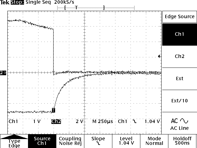
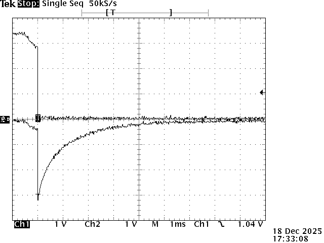
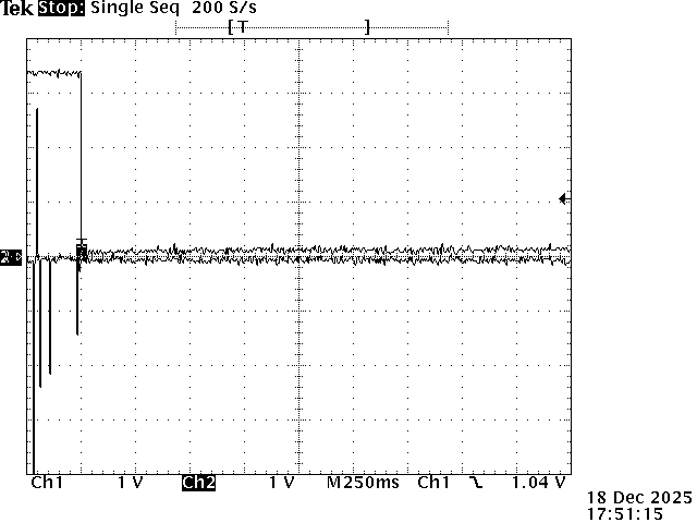
I am using the TPS63700 to generate -5 V, but the output is not designed to discharge the converter output when the converter is disabled. This function is added with an external RC circuit that enables a P-channel transistor to discharge the -5 V converter output to 0 V in order to get proper sequencing relative to other power rails. However, in some case this scheme partially fails, and part of the problem seems to be that the timing for disabling is not described in the datasheet.

In the external circuit a capacitor (1 µF) is connected between EN and gate, while a resistor (10 kohm) is connected between gate and ground. The drain of the P-channel transistor (DMG1013UWQ) is connected to the -5 V supply, and the source to ground.

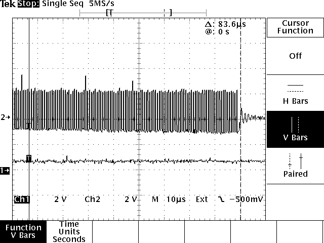
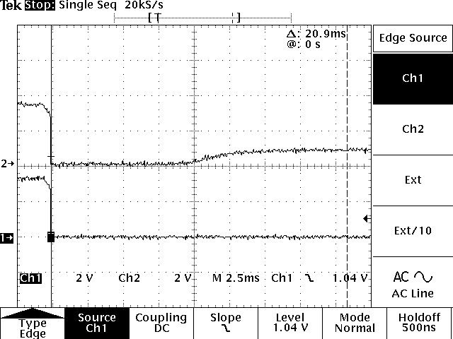
The rising edge of EN will enable the converter, while the capacitor will slowly charge (time constant 10 ms) to the voltage of the EN signal relative to ground. Much later the falling edge of EN is supposed to disable the converter and pull down the gate of the transistor (via the capacitor) thus letting it conduct and discharge the -5 V supply to ground until the capacitor is discharged to ground.

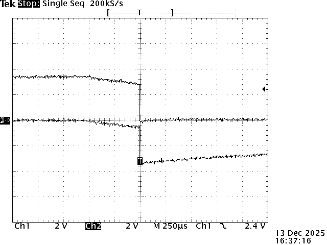
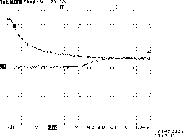
One board works just fine, but another partially fails as the output voltage immediately is pulled from -5 V to 0 V, but then after 16.5 ms the output unfortunately partially reverts to -920 mV. If the resistor is changed to 100 kohms, the problem disappears. I suspect that the converter in some cases is a little slow to turn off. Any thoughts?

I failed twice submit the above with the Edge browser but am trying Firefox now.

  • Hi,

    Our AE will give you feedback these two days. Thanks for your patience.

    Aurora

  • Hi Ole,

    Can you share your schematic? It's a little hard to understand your circuit without any schematic. 

    Best Regards,

    Travis

  • Did the schematics page get across? BRE, Ole Møller

  • Hi Ole,

    EN is driven by the buffer from the AND gate so I guess Q3 would have a very fast turn-on during EN off. So it's quite normal that there'll be LC ring on the Cout and parasitic inductance of the discharge loop. If the ringing didn't stop before Q3 turns off, there might be voltage left across Vout. Please try adding 5ohm on R39 and see if the problem still occurs

    Best Regards,

    Travis

  • Hi Travis

    I tried to go back to 10 kohm for R46 just to ensure that the old error was still there. Then I tried to change R39 to 10 ohms (didn't have 5 ohms lying around), but the problem still persisted. I suspect that it is the current in the inductor L5 (4.7 µH) that must go though the diode instead of ten the DC/DC converter when the latter is disabled, and that it is the associated energy that must be dissipated in the diode D27, transistor Q3, and resistor R39 (e.g. 5 ohms or 10 ohms). It looks to me that I need a large RC time constant to dissipate this ebergy so R46 (by experiment) should be more like 100 kohms rather 10 kohms.

  • Hi Ole,

    I ran simulation on this and C67 should be discharged much slower than VCAT. Can you share the waveform of EN, gate of Q3, and VCAT? trigger EN falling edge to capture the moment when EN turns low. use 200us/div as time scale

    Best Regards,

    Travis

  • Hi Travis

    I managed to get three shot for you. It seems that I can only attach one at a time.

    TEK00003.bmp:

    Ch1 (top): SAFE_EN_VCAT from the AND-gate disables the converter when falling (used as trigger).

    Ch2 (bottom): /DISCHARGE_:VCAT from RC midpoint goes negative and enables the PMOS transistor. It slowly discharges (RC = 1µF*10 kohms).

  • Hi Travis

    TEK00004.bmp: Here the top trace is from the previous shot (TEK00003.bmp), while Ch1 and Ch2 below are new:

    Ref1 (top trace): SAFE_EN_VCAT from the previous shot (TEK00003.bmp).

    Ch1 (middle at left): /DISCHARGE_VCAT

    Ch2 (bottom at l eft): VCAT (nominal -5 V)

  • Hi Travis

    I may have missed TEK00003.bmp. Here is a copy.

  • Hi Travis

    TEK00006.bmp: 

    Here the falling edge of the SAFE_EN_VCAT signal is used as external trigger (T, like in TEK00003.bmp).

    Ch1 (with spikes): SW output of converter.

    Ch2 (lower trace at left): VCAT (nominally -5 V)

    It seems to me that the inductor L5 (not a parasitic) and the output capacitors C49-C53 form an LC circuit, whose oscillations (as suggested by you) are triggered by the cutoff of the transistor and are only dampened by the Schottky diode. Before cutoff the current is already lowered by the diode D27, the transistor Q3, and resistor R39 (now 10 ohms).

    I suggest changing R46 from 10 kohms to 100 kohms, where earlier experiments have shown the problem to disappear.

  • Hi Ole,

    The other waveforms looks good. It looks like your circuit discharges the VCAT normally as expected. The problem is that the IC seems to be switching again. The sample rate is too low so we cannot see the details of the SW voltage. But I suspect there's switching behavior here:

    So can you help zooming in this moment to 20us/div with higher SR rate? Please add EN signal so that we can see whether it's enabled again.

    Best Regards,

    Travis

  • Hi Travis

    Here are the waveforms for EN (Ch1) and SW (Ch2) with VCAT falling edge at -500 mV used as external trigger (i.e. where the transistor stops conducting).

    Surely, looks like your suspicion with respect to EN (close to 0.9 V) was correct.

    The net SAFE_EN_CAT is supposed to be driven by the AND-gate (U9B) output, and I suspected that the gate failed driving the output to a low level when its supply voltage is very low. Thus I wanted to check whether the other half of the dual AND-gate (U9A) that shares the same supply has the same output behaviour at very low supply voltage. This gate has inputs PG_3.3V and PG_1.8V, and output PG_POS_B (received in cathode_supply.pdf to the left). The waveforms below are PG_POS_B (Ch1) and EN (SAFE_EN_VCAT) (Ch2).


    To me it looks like both AND-gates are capable to drive both signals to 0 V as they should, but that something else later is driving the net slowly to around 900 mV V just starting10 ms after the 3.3 V and 1.8 V are out of spec. This could point to the RC-cicuit with its constant of 10 ms. I suspect that the capacitor (C67), when the the AND-gate presumably goes high-Z, goes from 0 V on its left side and, say, -900 mV on its right side to +900 mV on the right side and 0 V on the left side, thus potentially restarting the converter.

  • Hi Ole,

    I'm not the expert supporting the logic gate. But from my understanding most CMOS logic gate uses push-pull output which should not output high Z during normal operation. Can you check the AND gate power supply waveform? If the power supply voltage does not drop below the AND gate supported supply voltage range, then you need to submit another thread with the part number of the AND gate.

    Best Regards,

    Travis

  • Hi Travis

    Here are waveforms for 3.3 V (Ch1) supplying the U9A/B dual AND-gate and the output (Ch2) of the AND-gate U9B when the power +5 V to the board is turned off. The trigger is the falling edge of the output corresponding to the EN signal of the DC/DC converter. The output is also connected to the capacitor, which I suspect raises the voltage of the EN signal, when the AND-gate ceases to function.

    Luckily I saw your response above as the usual notification e-mail never showed up.

    For R46 = 100 kohm, i.e. RC = 100 ms:

    For R46 = 10 kohm, i.e. RC = 10 ms:

    Thank you for your help.

  • Hi Ole,

    I think your assumption is correct. The correct time sequence should be :Cout discharge finish-> C67 discharge to 0 -> Power supply of the AND gate drops. But now C67 drop slower than ADN gate power supply, which means the AND gate cannot pull C67 to GND. and EN signal is pushed high again by C67. So the solution would be increasing the capacitor on AND gate power supply or reducing RC parameter on C67.

    Best Regards,

    Travis

  • Hi Travis

    I also got the idea this morning to reduce the RC parameter. With R46 at 1 kohm things look right as can be seen by the waveforms below that all trigger on EN (Ch1) going low. Thank you very much for your help and patience in getting a good and clean solution.

    EN and VCAT (-5 V)

    EN and /DISCHARGE_VCAT (Q3 gate)

    EN and SW

    BR, Ole Møller