


Hi,
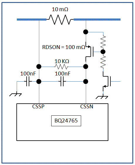
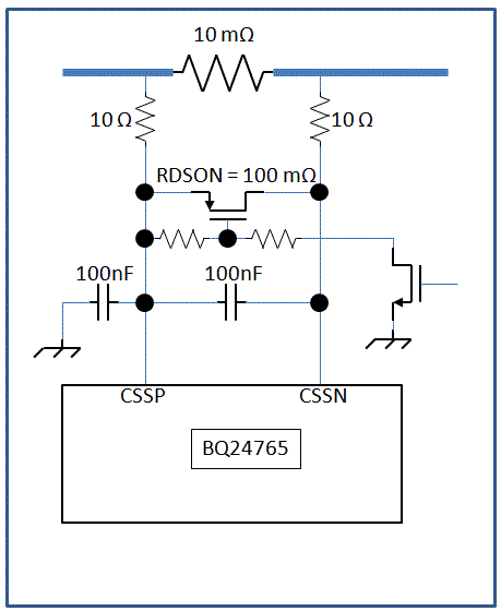
Attached to this message 2 schematics to shunt Rsense of input current (as explained in application note : slua533). We want to use BQ24765 because it integrates the 2 MOS and we need to save PCB area for our board. We want the battery charger to operate in autonomous mode (without a host) with a smart battery (SBS compatible). That is why we need to shunt the sense resistor.
- First schematic uses a PMOS in serie to cut the path to CSSN input of the differential amplifier : when this MOS is OFF, no current flows through the 10K resistor, and the battery charger measures 0V between CSSP and CSSN : charge of the battery can be done. When the MOS is ON, the CSSN input is plugged to the 10mohm sense resistor, and as a little current is flowing through CSSN input, RDSON=100mohm can be neglected : the input current limitation can occur.
- The second schematic uses two 10ohm resistors before CSSP & CSSN inputs. The PMOS then shorts both inputs when it is ON, and as RDSON=100mohm is little compared to 10ohm, the differential voltage is almost 0mV at the inputs, allowing the charge of the battery. When the MOS is OFF, CCSN & CCSP are no longer shunted, allowing the input current limitation to occur.
What are the drawbacks of these 2 solutions ? For me, the 2nd solution may induce measurement error due to the 10ohm resistors that will lead to gain error of the differential amplifier. That is why I would prefer the 1st solution. Do you think stability problems could appear when the MOS is ON and when current limitation occurs ?
Thanks for your answers.
