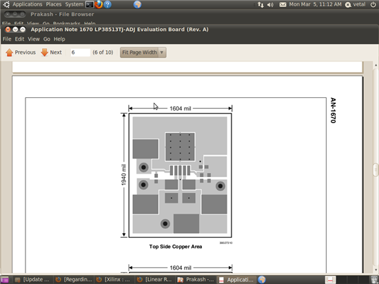
Dear Sir,
I am planning to use LP38513-adj regulator for 3.3V and 1.2V. Please recommend the appropriate heat sink model for this regulator to place in the PCB.
Thanks,
V. Prakash
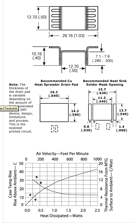
Dear Sir,
I am planning to use LP38513-adj regulator for 3.3V and 1.2V. Please recommend the appropriate heat sink model for this regulator to place in the PCB.
Thanks,
V. Prakash