This thread has been locked.

If you have a related question, please click the "Ask a related question" button in the top right corner. The newly created question will be automatically linked to this question.

UCC28061 / UCC28063 spontaneous gatedrive turn-on after turn-off

Other Parts Discussed in Thread: UCC28060, UCC28061

I'm working on a 10 KW 2-phase BCM buck converter based on the UCC2806x but got stuck. I've 'folded' the math and ins/outs so it works for buck application, and the circuit is working quite happily for a range of in- and outputvoltages. For any other range, strange things happen. This range is not clearly defined, but lies in the range of Vin=2xVout. Above and below is no problem (30KHz switching freq. works just as nice as 120KHz)

What happens is that immediatly after the gate driver (IRS21850 single high side) is turned off and current starts falling, the controller turns the gate on again, thus ramping current further up until it hits the current limit of the lab supply used. Most of the time the gate drivers don't survive. The same thing happens when GDB is disabled, when VINAC, VSENSE and HVSEN are externally controlled and when seperating  or not seperating PGND and AGND.

I've looked at it with a few colleagues, redesigned grounding and signal routing and ruled "everything" external out. The feedback may not look stable, but this is pickup. Gate B is completely disabled and remains so, even when A decides to turn on. When connecting gate B to Comp, the controller works fine until A starts misbehaving and then chaos happens, as can be expected. So, for tests, i've disabled B.

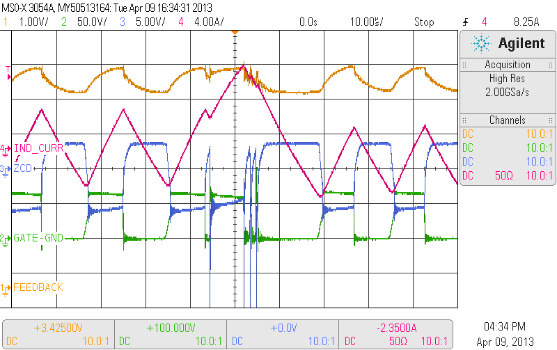
Green = Gate of MOSFET A vs GND (so a bit dirty, sorry for that, we've not kept every screenshot)

Blue = ZCD winding of A vs GND before RZCD

Purple = IL,A

Then we have (different scope, different day)

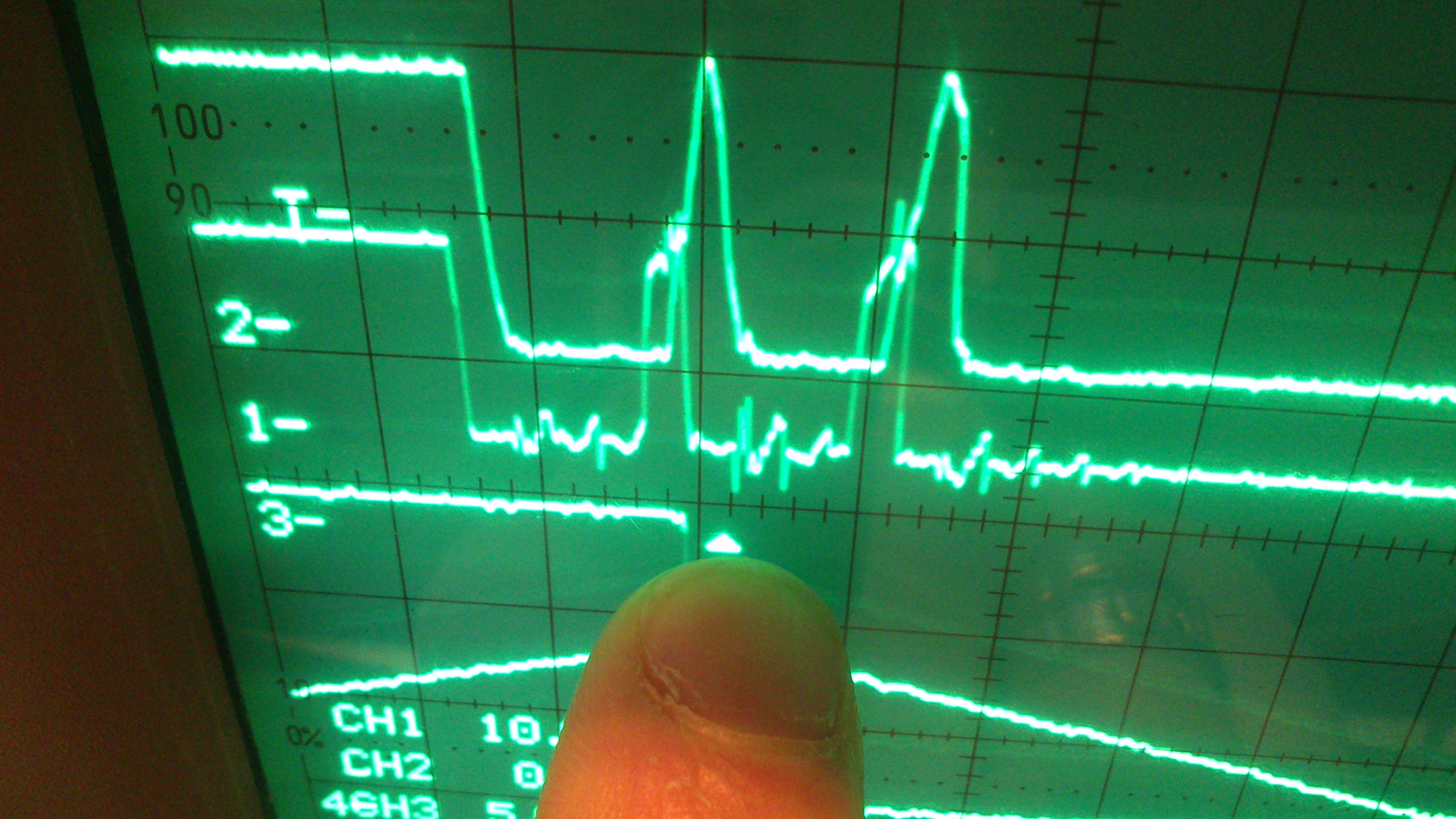
Top: VGS (diff probe) MOSFET

Bottom : output of Controller GDA

Clearly, the controller is first to turn on again. Not the FET, not the Driver, not the Current Sense winding, but the Controller itself. I've got more scope shots of all the other signals to reaffirm this statement.

I could list everything i've done, but in the beginning there was almost no decoupling and/or limiting switching speed and long wires. Now everything is limited, filtered and built on the controller itself. I've used other power supplies, coax or twisted wire. I've also eliminated reflections and ground bounce from controller to gate driver. All signals, supplies and ground became cleaner and cleaner, but no difference in behaviour.

Why does the controller decide to switch on again, with no apparent external cause?

  • I've added some extra Y-caps and it's stable across 30-130KHz. Sadly, still violent spontaneous switching.

  • i've now minimized the layout and came to the conclusion that when the controller decides it wants to turn on phase B again (turning B off and running on phase A works fine), it also fires phase A simultaneously. I can recreate this behaviour when controlling PHB externally. on the trip-point voltage where B should join in, phase A fires again, resulting in very large currents. The controller doesn't return to stable dual phase operation at all.

    Anyone?

  • Hello Floris,

    Look for noise or interference coupling into one or both of the ZCD inputs.  A noise "glitch" on these inputs can prematurely turn ON a gate-drive that normally should be off. 

    In an ideal environment, the ZCD inputs work like this:
    When the on-time for GDA, for example, is completed and the Phase MOSFET is shut off, the current inthe inductor demagnetized and the ZCDA voltage swings positive during this demagnetization time.  When ZCDA rises above the 1.7-V threshold, it "arms" that phase to turn on again once the zero-current detection (ZCD) crossing happens.  This crossing is defined as when the ZCDA signal swings back negative and falls below the 1-V turn-on threshold. 

    The ZCDx signals are usually derived from sense windings on their respective inductors (often relatively remotely located from the controller).  In the real world, the windings or the signal-track loop can pick up switching noise either from the other phase or from some other nearby power circuit.  If this noise is large enough, it can drive the ZCD signal below 1 V and turn that phase on before it should.  I think this is what appears to be happening in your system.  Phase-B's turn-on switching couples negative-going noise into ZCDA and triggers GDA to turn on again before its inductor has demagnetized.  This problem can exist for either Phase A or Phase B or both at the same time.  Careful signal routing is necessary to prevent this, including running the GND return for each ZCD winding back to the IC on a separate closely-spaced track parallel to the signal track.  Avoid connecting the ZCD-winding GND directly into a convenient nearby high current return path, which are often near the inductors and some distance from the quiet IC GND. 

    The ZCD inputs use current-limiting resistors in series with the windings, and a small capacitance to adjust the ZCD timing.  Avoid increasing these cap values for better "noise filtering".  They are not filters, but are intended to precisely set the turn-on timing to implement BCM (or as TI calls it: Transition Mode - TM).      

    I hope this helps you to debug your system.

    Regards,
    Ulrich 

  • Hi Ulrich,

    Recently we've found cause and solution. To remind everyone reading: i'm using this PFC controller in a BCM Buck converter application.N-MOSFETS are high-side, source at output & inductor side.

    There appeared to be one problem, but there were actually two.
    - The first one is described above (even when PHB disabled, phase A goes in spontaneous CCM)
    - The second one looked to be the same problem (phase A going in CCM) but wasnt.

    The first problem got solved when lowering the dV/dT-limiting capacitance and replacing the driver with a combination of a much more robust IR2113 as levelshifer + TC4452 as current driver. The original IRS21850 was exceptionally sensitive for negative gatedrive signals, and was creating havoc at the controller, triggering resets etc.

    The second problem exhibits the same behaviour, but did not occur with PHB disabled.This post is about how the second problem got solved too.

    ---It appears that when the controller tries to turn on phase B, it also switches phase A simultaneously on. This also happens with artificially induced (or none for maximum Tper) ZCD, VSENSE,  VINAC/CS at a fixed "OK" level and externally forcing PHB to trip between one and two-phase mode. I've made some 'scope printscreens and can post them monday if you want. Only after the first ZCD comes, phase-shifting starts. If no ZCD comes, simultaneous restarting continues. This behaviour is a fact.

    This behaviour is strange on itself, but should not be as destructive as it is. However, i've made a mistake in my bootstrapcircuit where phase B cannot create a bootstrap-supply. Both MOSFET sources are connected with eachother through the inductors and because of that, when the output is at anything higher then 0volts, phase B can never restart. Thus, with the controller restarting over and over, phase A goes fully CCM with destructive results.

    Previously, we've never checked if the MOSFET from phase B actually did turn on when going from single to dual phase, because clearly it worked when starting in dual phase mode (because both MOSFET sources were at 0 volts when starting!). The only thing we saw was phase A and B working perfectly as they should, then disabling phase B,  then trying to turn phase B back on and then phase A going full CCM and blowing its driver and/or controller.

    When ensured phase B could actually turn its MOSFET on by using a charge pump, this phenomenon never returned. Phase transition  now works as nicely as it should. I know the true pupose of the ZCD resistor/capacitor network.

    So both problems now seem to be an user fault and/or wrong choice of components. For now, only one question remains.
    - why does the controller turn on both phase A and B at the same time when transitioning from one to two-phase operation?

  • Hi Floris,

    That is an intriguing use of the PFC controller to operate in a buck topology.  Certainly some unexpected issues were bound to surface, and I'm glad you were able to find and debug them. 

    The UCC28060/61/63 series of interleaved controllers use a phase-locked-loop to maintain the 180-degree phase shift between each output.  Since transition mode (boundary conduction mode)  results in widely varying switching frequencies, the PLL continually adjusts the on times for each phase to stay 180 degrees apart. 

    However, the PLL needs to acquire the phase relationship before it can adjust it, so the initial start-up of the two phases start at the same time and the PLL is able to shift them to 180 after a few cycles.  This happens in 4 situations: at initial start-up, when Phase B is re-enabled using PHB input, recovery from an over-current event, and if the ZCD signal is lost.

    All 4 cases are related to the ZCD signal.  The PLL uses internal gate-drive signals, not ZCD, to effect the phase shift.  But there will be no gate drive for an output if there is no preceeding ZCD input signal.  At start-up, there is an internally-generated start pulse for both phases reccurring at 200us intervals.  Once the phases start swtiching, they generate their own subsequent ZCD signal necessary to trigger the next switching cycle, consequently: TM (BCM) operation.

    When PHB turns Phase B off, its ZCDB signal is lost, so when PHB is toggled high again, the internal logic starts it in-phase with Phase A and the PLL shifts them to 180 in a few cycles.   
     If an overcurrent condition is detected at the CS input, both phases are immediately shut off and stay off until the CS input voltage drops below 15mV to ensure that the inductors are substantially demagnetized.  The restart ends up in-phase again (see page 19 of the UCC28061 datasheet and page 30 of the -063 datasheet).

    Finally, in the case of instantaneously low output voltage (due to excessive ripple or heavy load step), if the peak of the highest high-line approaches too close to Vout there may not be enough voltage difference developed on the ZCD windings to cross the input thresholds necessary to trigger the next gate-drive pulse.  Switching stops and does not resume until an internal automatic start pulse occurs after 200us.  If the ZCD voltage is still inadequate, you can see a series of restarts about 200us apart until the output-to-input voltage difference increases enough to restore the proper ZCD signal level and maintain next-pulse triggering.   The PLL can then restore the 180 phase shift as well.

    So the in-phase start-up behavior is a fact, as you say, although temporary and brief.  I hope I've explained why and when this can occur.  I'm not sure if there are any other ramifications when operated in a buck topology.  I hope you've found all of the nuances involved with adapting the PFC controller to interleaved buck convertion and enjoy smooth progress to production.

    Regards,
    Ulrich 

  • Dear Ulrich,

    A quick question: what is the on-time right after the restart? How is it determined? In the SLUS837A datasheet for UCC28061, page 6, note 4, only a brief mention is made on this. I noticed the on-time varies (with input voltage) but there's no explanation on why or how this so. Is there any way to estimate this on-time and which input does it depend on?

    Thx.

    S.K.
  • Hello S.K.

    The theoretical operation of these Transition-Mode (TM) PFC converters is based on constant on-time for a given load level. The input voltage varies from zero to peak but each switching cycle's on-time is the same, and with TM-boost the result is that the average input current follows the input voltage.   The maximum on-time is set by the value of the TSET resistor, calculated using equations on page 16 and 17 of the DS at the maximum output power and minimum input line.

    The on-time is modulated by the magnitude of the COMP voltage, which is maximum at full power, low line, and reduces as load decreases and line goes up. Therefore, the on-time you may expect to see for any particular restart event depends on the max power setting (by TSET resistance) and the value of the COMP voltage at the time of restart. 

    However, there is one more variable that is not part of the general theory, but is a modification of on-time to improve cross-over distortion near the input zero-crossings.  When the input voltage is very near zero, little current can build up in the boost inductors during the normal on-time.  The result would be flat-spots in the current waveform at the zero-crossings. The UCC28060/61/63 family incorporate a cross-over distortion reduction feature which adds additional on-time depending on how close to zero volts the input is.  Figure 23 on page 15 indicates the amount of additional on-time added to the normal "constant" on-time programmed by COMP, based on the scaled input voltage seen at VINAC.  This non-linear curve adds considerable on-time near zero and reduces quickly above 0.5V.        

    So, again, the on-time you might expect to see at a restart depends on the COMP voltage at the time of restart and the maximum time programmed by TSET, and how close to zero VINAC is.  This can be estimated for the different line and load conditions by calculation, using Rtset and the COMP and VINAC voltages.

    Regards,
    Ulrich

  • Hi Ulrich,

    Many thanks for your reply. It explains why the on-time changes with the input voltage.

    One additional question: are the on-times during restarts different between phases A and B? In my case, the phase A on time is ~ 50us whereas that of phase B is only ~ 15us. Tset is 330k, which implies a Kt of ~ 10us/V. Vcomp is consistent at 2.4V and VINAC is stable at 3.5V (out of the additional on-time range?) VSENSE and HVSEN are tied together at ~ 1.8V (36uA source turned on) an PHB is tied to VREF at 6V (2 phase operation). Although, there's no MOSFET tied to the gate outputs, Vcs floor noise is below 20mV. Is there any additional handle that determines the restart on-time?

    Thank you.

    S.K.

  • Hello S.K. 

    You are correct, there is an additional factor to the on-times during the restart sequence that I forgot about.  During steady-state operation, the phase relationship is held close to 180 degrees by a phase-locked-loop (PLL) which uses the ZCD inputs for phasing information.  Under dynamic conditions, the PLL slightly adds on-time to one phase and subtracts from the other (in either direction) as necessary to maintain the 180 relationship.  At a restart, the PLL is skewed to one extreme, so one side has significantly more on-time than the ideal, and the other side has much less.  Per the given parameters, one would expect ~22.6us on-time for each phase once steady-state operation is achieved, and VINAC > 2~2.5V. 

    It appears that the pre-start on-time skewing is asymmetrical from the target, but the proper phasing and timing is usually achieved within several switching cycles of restart.  I can't account for the asymmetry of skew from the ideal, but I would imagine that either the short time stays short until the long time reduces to the symmetrical point and then they converge together, or that the long skew convergences faster to the ideal target than the short skew does.

    Looking through the UCC28061 datasheet I noticed that there is a graph of on-time ratios relative to phase shifts with Rtset as a parameter, shown as Figure 21 (page 15).  An obscure factor to the skewing could be due to the high value of Rtset (330K).   This is a difficult graph to understand, but I believe it may have some bearing on the question.  The PLL generates an error signal which is used to adjust the two phase on-times appropriately.  As such, the error is finite so some small phase shift from ideal 180 is inevitable, and this error appears to have a greater impact with higher values of Rtset.  I don't know why.  But per the graph, a higher phase shift error results in an on-time ratio Kt/Kto which applies inversely to each phase on-time with respect to the ideal on-time.  This suggests that the high TSET resistance is contributing to the asymmetrical skew of the restart on-times.  And certainly, there is maximum error in the PLL output at the moment of restart, where the two phases start at zero degrees.  It is not clear if the curves maintain a relatively linear relationship out at the extremes of phase shift, and maybe some internal circuit limits are hit before then, but I wonder if understanding the trend is more important than accounting for the exact numbers.  

    I hope this helps to clarify the on-time behavior that you are seeing.  I'm sorry that I missed these points the first time.

    Regards,
    Ulrich 

  • Hi Ulrich,

    Many thanks for your detailed explanation. I forgot to mention that both phases fire at the same time as pointed out by you.

    I have trouble with erratic startups under full load with this asymmetry because the overcurrent sensing will cut off the high Kt phase prematurely while the low Kt phase is too short. As a result, there's not enough voltage to kick in the zero crossing (1.68V) and change the PLL error signal.

    Maybe one way out is to reduce the TSET resistance, but I wish to keep it at 330k in order to cap the maximum switching frequency to ~ 180kHz. Is there anything I can do to the TSET input in order to reduce this asymmetry, at least during start up? I'm guessing that putting a series RC in parallel to the RTST resistance harm the operation could work, but to be sure, it would be nice if you could shed some light on the internal mechanics of this specific pin.

    Thank you again.

    S.K.

  • Hi S.K.

    I apologized for my delayed response.

    A simplified explanation of the on-time generation is that a matched set of capacitors are charged up at a linear rate (constant dv/dt) with matched current sources. At the beginning of each on-time, each phase’s gate-drive output is driven high and its respective timing capacitor (having been previously discharged) is allowed to charge up. When it reaches a threshold set by the COMP error voltage, plus any other special modifications to the on-time, the gate drive is driven low. The PPL manages the timing of each phase to keep them interleaved at 180 degrees. Each of the charging currents is proportionately mirrored from the current established out of the TSET pin to GND.

    The TSET structure is basically a source-follower which regulates the voltage at TSET to about 2.6 V and the resistance to GND establishes the reference current. For the usual boost-PFC application, higher Rtset means lower current, slower charge up, longer on-time and higher output power (provided that it is not limited by other mechanisms, such as current limit, etc.), and lower Rtset means the opposite. So for a given boost inductance and input voltage, lower Rtset will program less on-time which reduces the maximum deliverable output power.

    But if I assume correctly that you’re using this in a non-typical BCM buck configuration, as at the start of this thread, I’m not sure about the timing considerations. At start-up, a discharged COMP voltage should act as a “soft-start” and gradually increase each on-time from near zero. But as I envision it, Vout = 0 V, and Vin can be quite high, so di/dt charging the inductors will also be quite high. It may be that the COMP slew rate at start-up is too fast to keep the peak current under control below the current-limit threshold. This may be the case even if you try to temporarily reduce Rtset to reduce the maximum allowable on-time. The circuit to temporarily alter Rtset may increase its susceptibility to noise on TSET which can have an erratic effect on the normal TSET current, which in your case is about 8 uA. (By the way, do not add any direct capacitance to the TSET pin “for filtering” because the noise currents in this capacitance will drastically interfere with the uA-level dc current normally expected here.)

    I suggest to implement an artificial soft-start circuit that attaches to COMP (maybe through a Schottky diode) and keeps it rising very slowly to give the output a chance to build up while keeping the on-times (and peak currents) low. After a point, the artificial soft-start can rise up above the COMP voltage and be effectively disconnected by the back-biased diode (or by some other means).
    If you are starting into a full load, this may complicate things because it makes it difficult to build up output voltage, unless the load is delayed until a suitable output threshold is reached.

    Regards,
    Ulrich