


Design Parameters: Vin: 14V DC / Vout: 5.2V DC / Iout: 4.2A / Ta: 50degC / Max Tj: 100degC / 2-layer PCB
Interpolating between Vin of 12V and 16V, and between Ta of 25degC and 85degC on the LMZ12008 data sheet, I get efficiency of ~90% and Pd of ~2.4W. Plugging Pd into formula 13 on page 18, I get Theta CA of 19.83degC/W.
Moving to page 5 of AN-2020, formula 6 produces a Pd of 2.43W (Theta CA of 19.58degC/W), which agrees closely with the data sheet. Looking at formula 9 (page 6), and using the more conservative value from formula 6, I get a board size of 5.76in2. However, formula 11 (and formula 15 on the data sheet) produces a much different result: 3.96in2.
My questions:
1. The example in AN-2020 paragraph 3.1.1 produced board sizes that differed by only 0.030in2, but mine are much farther apart. Which calculation above produces the correct minimum board size?
2. Do these calculations assume a 2 or 4-layer board?
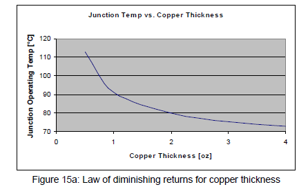
3. I've been unable to find a formula or rule of thumb for using 1oz copper vs 2oz. Is there any reliable guidance on this, beyond AN-2026?
4. Looking at AN-2020 paragraphs 3.2 and 3.2.1, how do I apply the effect of a thermal via array to my calculation of minimum board size? Is it directly additive to Theta JA, producing a proportionately smaller board? The first paragraph on page 19 of the data sheet seems to suggest that it's built into the calculations and thermal vias are simply best practice, with no "reward" (smaller board) for using them.
Thanks,
Eric


