This thread has been locked.

If you have a related question, please click the "Ask a related question" button in the top right corner. The newly created question will be automatically linked to this question.

Mosfet Switching Low Dropout

Other Parts Discussed in Thread: MAX3223, CSD23381F4, CSD25481F4, CSD25483F4

I'm having some troubles using Mosfets as switches.

The main idea is that i have to Turn ON/OFF some circuits as a Flash Memory, Leds, MAX3223, an so on; i have 3.3V to feed all the circuits which are controlled by a Microcontroller.

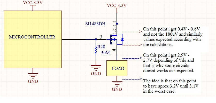
By this way, my problem is that the Voltage Drops over 300mV and more and some IC doesnt work correctly. Because for example, at the Drain pin of the Mosfet is not 3.3V  if not 2.9V and this is unuseful.

I would like you help me to resolve this,  a way where the dropout doesnt be greater than 0.1V 100mV.

Thanks For Your Help!

  • Ricardo, 

    If I am understanding you, you are saying that the Drain to source voltage across the MOSFET is too high when the FET is on. The first question I have to ask is what gate voltage are you using to drive the MOSFETs, and are you sure that they are fully enhanced? 

  • Yes, you know what i mean. I'm using the 3.3V from a pin of the Microcontroller as gate voltage (LCD ON/OFF - FLASH ON/OFF).

     Sorry, I dont understand what you mean with Fully Enhanced?

    My problem is complex because i'm using Batteries and the dropout (Drain to source voltage across the MOSFET) is about 400mV and if the batteries fall so much (3.3V-0.4V=2.9V), some circuits could not work in shortly time.

    Thanks again Brett,

    Regards,

    Ricardo

  • Ricardo, 

    What voltage do you have driving the gates of the FETs? There should not be that much voltage drop across the FET. 

    What FET are you using? It'd be great to have a datasheet. 

  • Hello Brett,

    Im driving the FET with 3.3V.

    I had not attached the datasheet because is not a Texas Instruments MOSFET, but it is a N Channel (si1488dh). I attached the Datasheet. 0636.Mosfet Canal N (si1488dh).pdf

    I hope not be a problem and that you continue helping me with me.

    Thanks again,
    Ricardo

  • Ricardo, 

    Looks like 3.3V should be more than enough to completely turn on (or fully enhance) the device. 

    The next important question is how much current do you have running through the FET? 

  • Brett,

    The current across Drain-Source depends of the circuit load, for instance, with the Flash memory is 4mA when is running.

    Now, i have a question, if the FET is fully enhanced the Drain-Source voltage should be of?

  • Ricardo, 

    Not entirely. Because of the internal Rdson of the FET, some voltage drop will still be required. 

    But if you refer to the figure on the top left of page three (output characteristics), driving at 3.3Vgs, you shouldn't require anything more than roughly 100mV Vds to achieve up to at least 1A of current. 

     If you were driving lots of current, I'd say you might need to parallel FETs but this is not the case. 

    Can you get a reading of the on resistance of the FET when it is turned on? It should be somewhere in the range of 45mOhms. 

    (V=I*R=4mA * 45mOhms = 180uV so this is in the proximity of the voltage drop across the FET that we would actually expect)

  • Thanks Brett!!!

    I did what you told me and i got values of ON resistance of 150 mV and some approximates depending the circuits.

    Now i attached an image in order to explain it better. Which could be my problem? What could i do?

  • Hi Richardo,

    Have you consider to use LDO like LP2980AIM5-3.0 which has enable pin and has low dropout voltage- for 10mA load it doesn't exceed 90mV.

    The price will not significantly differ from  SI1488dh but with LDO your voltage will not depend from load current.

  • Hello Oleksiy,

    Thanks for your collaboration and it looks great but i'm sorry, i haven´t said that some circuits could have Current Peaks of 3A so that LDO couldn't works fine.

    Now, one of the most important points of this project is save power as better as possible and once the LDO is turned on it will consume a little more current.

    Best regards,

    Ricardo

  • Ricardo, 

    I see your problem. You are driving the gate with 3.3V, and when the switch is turned off, the gate to source bias is 3.3V as there is 0V on the source. However, as you turn the device on, voltage on the source builds up and and the gate to source bias decreases. With Vcc on the load (tied to the source) and Vcc on the FET gate, the Vgs bias will be zero. Because you only require a very small current, basically you are driving the gate just enough with whatever that voltage drop is and its enough to somewhat turn on the device, but not completely. 

    There are a couple solutions. The most obvious is to drive the gate with a signal greater than 3.3V such that Vgs will be positive when you need it to be. However, if you are using just a microcontroller, this might not be possible. 

    Perhaps a better solution for you would be to use a P-Channel FET and invert the signal from the microcontroller such that the FET is off (blocking) when its bias is postive and on (conducting) when its gate signal is turned off. 

    It just so happens that the TI NexFET group has just released three small signal P-Channel FemtoFET devices that would be ideally suited for this application. 

    CSD23381F4

    CSD25481F4

    CSD25483F4

    I would direct you to try implementing one of these if you go with this option. 

  • According you told me, i have a big problem because i have 900 boards which each one have 9 Mosfets on this configuration. I didnt thought that my troubles were so complex.

    As you told me, i cant resolve my problem using another MOSFET, is to say, a MOSFET that has 6-TSSOP, SC-88, SOT-363 encapsulated???

    If not, i will try to change or stop the prodution of the boards and implement new circuits design. So could recommend me a circuit to implement what i would like to do? The P-MOSFET is not useful for me because i always must have a 3.3V or an 1 logical from the microconcontroller pin in the gate of the MOSFET to turn it off and there is always a consumption and remember that i am using batteries and I must have to save power as much as possible. .  

    Best regards,

    Ricardo

  • Ricardo, 

    You have three options as far as I can see. 

    1) I still do not see why you cannot send you micro controller signal through an inverter to easily turn on or off the P-FET. I do believe this is your best bet

    2) You could somehow boost the drive signal of the inverter to a value greater than 3.3V so that the gate to source bias on the FET is positive and will actually turn on the FET

    3) You could use a bootstrap configuration to drive up the gate signal to the FET . 

  • Thanks a lot  Brett!

    Now, I would like to know if you have other MOSFET with another package SMD, bigger than the FEMTOFET ?

  • Ricardo, 

    I will refer you to our NexFET P-Channel landing page.

    http://www.ti.com/lsds/ti/power-management/p-channel-mosfet-transistor-products.page?paramCriteria=no

    Admittedly, the selection is not huge - a great deal of the FETs are Chip Scale Package (CSP) devices and like FemtoFETs, they are very small. However, there are two QFN devices that may meet your needs, listed below. 

    CSD25302Q2

    CSD25401Q3

  • Thanks Brett!!

    I will take it in count!! Excellent your great help!