This thread has been locked.

If you have a related question, please click the "Ask a related question" button in the top right corner. The newly created question will be automatically linked to this question.

UCD9090 Programming

Other Parts Discussed in Thread: UCD9090, UCD90SEQ48EVM-560

For the UCD90SEQ48EVM-560 Development Board, I am interested in the actual programming when utilizing the Fusion Digital Power Designer programming GUI provided by TI.  Does the programmer program the power sequencer device (UCD9090) directly or does it require additional components in order to program?  Specifically, is the TSUB3210PM required as well?

  • Fusion Digital Power Designer mainly uses TI USB to GPIO Adapter to communicate with the UCD90XX devices on the EVM (below is the links).
    • If you have the EVM board => then connect the USB to the PC and the other end of the cable to the EVM board.


    http://www.ti.com/tool/usb-to-gpio
    http://www.ti.com/lit/pdf/sllu093

  • I am communicating just fine with the eval board.  I am asking from my design perspective where I do not have any peripheral components, just the UCD9090 and a PMBus interface to my edge connector. 

  • If you use Fusion Digital Power Designer to program the device, you need the USB-To-GPIO adapter. If you don't have the EVM board, then connect the device's PMBus CLK pin (pin #8), and PMBus DATA (pin 9),  to the adapter's SCL and SDA pin (J2, pin 9 and pin 10)

  • Hi Anne,

       I saw "Fusion software supports firmware development and downloading" in the introduction of Fusion software.

      1. In order to use UCD92xx, do I need to develop firmware for UCD92xx? or do I need to download TI's firmware   

           before using it?

       2. How can I configure UCD 92xx? Thru PMBUS/I2C, JTAG or both?

           if using JTAG, do I need BSDL file?

       3. Do I have to configure UCD parts each time after power up? or all configuration data can be saved to a non-  

          volitile memory inside UCD parts.


    Thanks,


    Tony

  • 1. You don't need to do anything. When you order the part, it already has firmware loaded. Fusion GUI support firmware download in case the users want to do firmware upgrade

    2. You can configure the device using both PMBus/I2C and JTAG. PMBus is preferred over JTAG.

    3. The device has non-volatile memory =>just save the configuration to the non-volatile memory, then you don't need to configure the part each time it resets.

  • Is there a way to verify what programming file has been loaded (i.e. checksum)?

  • If you use Fusion GUI, you can read the program flash checksum by using Memory Peek/Poke tool:

    1. Launch UCD3XXX / 9XXX Device GUI (Start menu -> All Programs ->Texas Instrument Fusion Digital Power Designer-> Device GUIs-> UCD3XXX & UCD9XXX Device GUI)

    2. Click on "DEVICE ID" link to scan for device, if device is in program mode, it will be discovered

    3. Click on "Memory Peek/Poke" link => Memory Peek/Poke tool will be displayed

    4. You can read the program flash checksum at address 0x7FFC (if device is in Program Mode), or at address 0x17FFC (if device is in ROM mode), checksum is 4-bytes data

  • The "Memory Peek/Poke" function is password protected.  How do I obtain this?

  • I will put a document together to explain what is needed, a password is not required to obtain the checksum via the method Anne has described.

    What she has provided will give you the checksum of the FW that is loaded in the device as it ships from the factory it will not provide you with a checksum of the configuration that the customer loads.

    The FW checksum will not change over time as the FW that ships with the device will not change and any new FW features/changes/updates are released as new P/Ns.

  • So is there any way to verify what is programmed to the device?

  • Has there been any progress in to verifying what is actually programmed into the device?

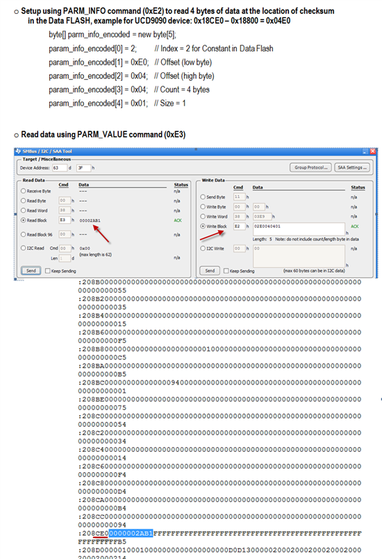
  • Data flash checksum for UCD9090 is located at memory address 0x18CE0. The Data Flash memory start at 0x18800 => Offset will be 0x18CE0 - 0x18800 = 0x04E0

    You can read the dflash checksum using either Fusion GUI or SMBus/I2C/SAA tool.

    1. Use Fusion GUI: From File menu->Export -> Data Flash file, select Intel Hex format, then export the data flash to the file. The checksum is located at memory 8CE0

    2. Use SMBus/I2C/SAA Tool and PARM_INFO (0xE2) & PARM_VALUE (0xE3) commands:

    •  Launch the tool, make sure to enter the correct PMBus address
    • Setup the memory address to read using PARM_INFO command(0xE2). In the tool, WriteBlock where cmd = 0xE2, and data = 0x02E0040401. The data comes from:
      • byte 0 = 0x02 // index = 2 for Constant in Data Flash
      • byte 1 = E0    // Offset (low byte)
      • byte 2 = 04    // Offset (high byte)
      • byte 3 = 04    // Count 4 bytes
      • byte 4 = 01    // Size = 1
    • Read data flash checksum using PARM_VALUE command (0xE3). In the tool, ReadBlock where cmd = 0xE3
  • I am trying to insert a hex file so that you can see what we were able to capture in the lab.  This tool is not allowing me to do so but I do not believe the above procedure using the Fusion GUI reading at location 0x04E0 is not working correctly.  Please advise how we can proceed discussing/viewing the results.

  • Could you also elaborate on the difference in your last response when describing the checksum location.  I see both 0x04E0  and 0x8CE0 as the location of interest.  Which one is it?  In the hex file I was able to generate, location 0x8CE0 is not an option.

  • The 0x04E0 is the offset from 0x18CE0 - 0x18800. The data flash check sum is at location 0x18CE0. You only use the offset when reading the data flash checksum using PARM_INFO & PARM_VALUE commands. If you use the hex file, check. Below is the image for reference. The top is the tool to read data flash using PARM_INFO & PARM_VALUE, the bottom is how to read the dataflash checksum in the hex file

  • My contact info is 505-828-6883 .  Could you please give me a call?

  • If you are using one of the TI provided tools, Fusion Digital Power Designer or Fusion Manufacturing Tool, etc., then you will need the USB-to-GPIO adapter to facilitate communication between the Windows host system and the PMBus interface of the UCD9090.

    But any SW/device combination that can write to the PMBus interface is capable of loading a configuration and it is also possible to load a configuration by JTAG.  The Export selection from the File dropdown of the Fusion GUI will produce a number of different file formats for configuration loading.  Refer to the document,  Configuration Programming of UCD Devices, which can be accessed from the Help --> Help & Documentation Center link in the Fusion Digital Power Designer GUI for more details on the available methods.

  • When I used Export->Data Flash Hex File from the Fusion Digital Power Designer I got a file with the header showed: DFlash Checksum: 0x02306F and I don't understand what this number means. Is it the UCD9090 program flash checksum? The version of my UCD9090 Firmware is v2.3.5.0.

  • Any tool from TI can program the UCD9090 data flash with the hex file exported from Fusion Digital Power Designer tool, instead of using TI Digital Power Manufacturing Tool with script file?

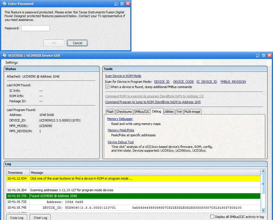
  • When I clicked the Memory Peak/Poke, it asked for the password as shown above. How can I get the password for this UCD3xxx/UCD9xxx Device GUI tool?