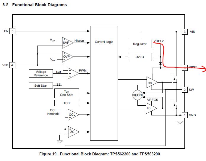
What voltage could be seen across the boost cap?
Assuming Vin is 12V, the wavefrom on the SW pin is 0 to 12V switching waveform. The VBST pin presumably has a voltage already on it, so that during the high cycle of SW, the VBST voltage can be pushed up for a source to bias the N-ch FETs. But how much?
If we're to allow for DC derating of ceramic caps, then the maximum voltage imposed across the cap is needed, so a cap of a suitable voltage rating and derating spec can be used.
The minimum required capacitance of the cap would also be useful. I didn't spot either of these in the datasheet (TPS62200).
Regards,
Lyndon