This thread has been locked.

If you have a related question, please click the "Ask a related question" button in the top right corner. The newly created question will be automatically linked to this question.

LMZ13608 - Saw tooth on the output

Other Parts Discussed in Thread: LMZ13608, LMZ14203

Hi,

I use the LMZ13608 on the board with 1.2V, 2.5V, 3.3V.

first batch was 3 cards.

In one of the cards , on the voltage of 1.2V, i get Saw tooth on the output of about 200 mv and every ~175 us (not the freq of the lmz13608 internal osc).

I read again the DS and didn't found any explanation except defect component.

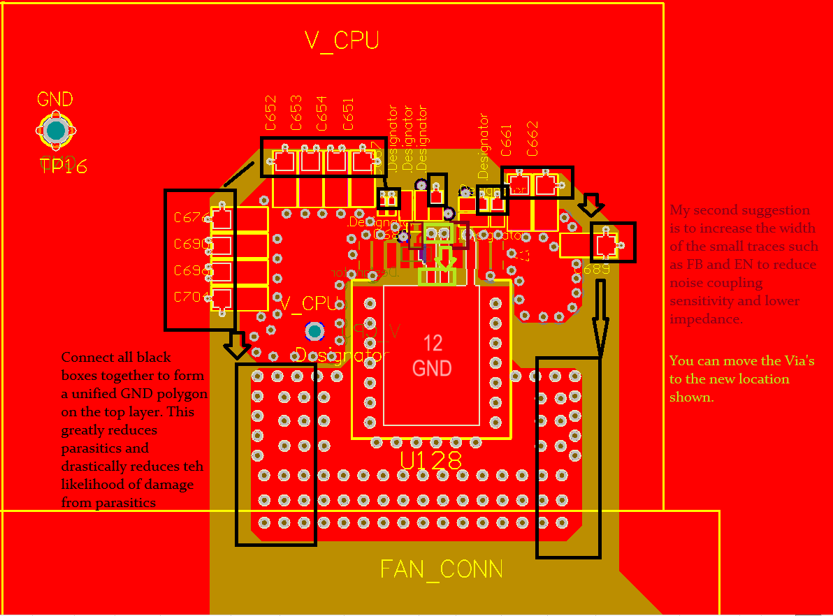
Imlementation (component name came from LMZ13608  DS):

cin: 3X10u+0.1U

Cout: 8X100U+4.7u+0.1U

Rfbt:: 1.033 kohm

rfbb: 2Kohm

css: 0.1u

Rent: 100K

Renb: 20K

Cff: was 10n and now is unmount (no change in the Saw tooth)

Pls advise

Regards

Zeev Gerber

  • Hi Zeev - To fully diagnose your problem, please send us a snapshot of your schematic and PCB layout and also include the VIN and IOUT conditions that you're testing. If possible also send us the scope shot of the "saw-tooth" waveform.

    Thank you!
    -JP
  • Hi,
    Attached link for schematic and PCB layout. The problematic voltage called V_CPU (1.2V used for CPU core).
    To open the shared files, click or copy the link below:
    data.gehealthcare.com/.../v.aspx
    Another update: The problem Disappeared when the LMZ13608 was replaced.
    The first step I ask you to do is check if you see some problematic/marginal values in the components serve the LMZ13608.
    I want to send the card for second phase production ASAPRegardsZeev Gerber
  • Hi Zeev,

    Thank you for the layout and schematic. We are evaluating it and will have a response for you tomorrow.

    Thanks,
    Anston
  • Hi Zeev,

    I am sorry to hear you are facing these issues. I took a look at the layouts and schematic you sent over and I've made suggestions here:

    It is also suggested to remove thermal relief from the pads of the passive components to minimize impedance and maximize conductivity.

    Did you do any impedance tests on the pins of the IC after you swapped it out? I would be interested to know if there is any change in impedance between the failing IC and a new one.

    Please also follow the suggestions in this document as pertaining to module soldering and design.

    Design Summary - LMZ1 & LMZ2.pdf

    This will help prevent over heating the module during solder rework and causing unintentional damage.

    Your schematic is correct and I see no cause for concern. Your layout with the suggested tweaks will make for a sturdy design and you should have no trouble going forward with second phase design.

    We only see issues like this, when an incorrect reflow temperature was used.

    Let me know how I can assist you further,

    Thanks,

    Anston

  • Hi Anston,

    thanks for your help.

    I check agaim the output of the DC2DC (3 units of lmz13608 and 1 unit of lmz14203)

    I find also Saw tooth on the output of the LMZ14203.

    it's exist on all cards.

    the amplitude is 50 Mv (1.195 to 1.245) and freq is ~80Khz (125 us)

    I attach again the SCH and also scoop screen shot.

    Pls. advise

    Zeev gerber


    To open the shared files, click or copy the link below:

    https://data.gehealthcare.com/fs/v.aspx?v=8b6c69885a60a078a398

  • Hi Anston,

    I change the Ron from 100K to 33.2K to make the Fsw faster (from ~100k to ~280K)

    I also checked the ESR of the Co and see that 5 units will have 6 mOhm ESR at 100K and  2 mOhm ESR at 280K.

    6 mOhm ESR with 1A not suppose to make 50 mv saw tooth.

    Happily  the magnitude of the saw tooth/noise reduce from 50 Mv to 20 Mv, resault which I could live with.

    Pls advise this phenomenon.

    In adition I think the DS of the devise should recomende on Fsw value to get optimum resault.

    Regards

    Zeev Gerber


  • Hi Zeev,

    I believe all the voltage ripple issues you are seeing are because of improper bypass capacitor placement. For U128 or V_CPU rail, the bypass capacitors C667 and C673 have traces instead of copper fills connecting them to the plane, more important however is the grounding. The grounds for these caps are Via'd through the board increasing the inductance and negating the benefits of the bypass capacitors.

    All the other capacitors on your design also have their grounds Via'd and very thin traces to GND. This amplifies inductances and causes ripple problems.

    Increasing the switching frequency will definitely reduce the output ripple magnitude since,

    where dc is the duty cycle.

    This equation was derived from here:  Additionally please check out this link which demonstrates how to accurately measure voltage ripple() .

    Thanks,

    Anston