This thread has been locked.

If you have a related question, please click the "Ask a related question" button in the top right corner. The newly created question will be automatically linked to this question.

What's driving the TIMER pin internally in the TPS24720 Hot Swap controller?

Based on very recent TI recommendations, we've eliminated the dV/dt MOSFET gate drive approach originally being used.  Not surprisingly, an oscillation is observed on inrush ramp-up, arising when the Vin DC supply enters CC mode at 2Amps with the inrush limit set to 10Amps.  When the supply is driven into CC mode as the MOSFET current slews up, Vin momentarily drops below the EN pin threshold, rapidly shutting the MOSFET down.  EN serves as the UV monitor for Vin through a divider network per the TI example application. When Vin recovers and again crosses the EN threshold, the MOSFET current slews up rapidly, repeating the cycle. The intentionally thin decoupling on Vin permits a short cycle time, observed to be around 6.2kHz.  This clearly demonstrates that the inrush current needs to be carefully chosen with respect to the capabilities of the source, and for hot insertion applications, the design needs to ensure the controller is enabled only after insertion is mechanically settled, requiring more than a simple divider network on EN.

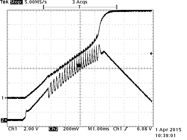
What was unexpected, however, was that the TIMER pin exhibited similar oscillation on its rising slope, displaying rise/fall edge rates that defy explanation by the functional block in the datasheet (Figure 5).  When the MOSFET shut down by EN, the TIMER cap discharged by about 200mV with a current far greater than 10uA.  When the MOSFET turned back on, the TIMER cap voltage also rapidly recovered the 200mV drop, somewhat slower than it fell but still far faster than expected from a 10uA charge current.  During this oscillation event, which lasted through much of the Vout risetime of around 6-8msec, the overall slope of the TIMER pin voltage remained monotonic but shallower than the normal linear ramp, roughly doubling the timeout limit.

During the investigation, the EN pin network was changed from a resistive divider from Vin to a long time-constant R-C filter without voltage division.  The oscillation disappeared, both on Vout as well as on the TIMER pin, with the Ct charge-discharge cycle exhibiting linear ramps as expected by the 10uA sources. It is apparent the the EN pin has an effect on the TIMER pin that is not fully explained in the datasheet. We are are looking for two answers from this post; 

First, explain how the TIMER Ct voltage can exhibit 6.2kHz 200mV pk-pk oscillation on a 47nF capacitor, from a pair of 10uA current sources.

Second, are there any simple example designs that take EN out of the Vin loop during inrush but still utilize it as a UV monitor function?  A larger hysteresis on the EN input comparator would increase its immunity to Vin transients, but there is no way of adjusting it.  R-C filtering seems to be the simplest option, but may prove troublesome on momentary losses of Vin.

  • Ricky,

    First off, your VIN supply should always have more capacity than the current limit trip setting in order to enable fully the protection features of the controller. Using dV/dt start up can ease the stress on the VIN supply during start up but once the normal current limit takes effect then an overload can crash the VIN supply and cause the controller to become disabled.

    The effect you described is common when the VIN supply is not adequate to support the loading after the hot swap (or the loading as the output capacitors are charged during startup).

    The TIMER does have the 2x 10uA current sources which are active in normal TIMER fault modes. The TIMER pin also has a 4.5mA sink current (2mA minimum) which becomes active when the EN pin is below the turn off threshold. So, for your case the ON-OFF-ON interaction between the VIN supply and the hotswap (and load) is causing the EN to cycle above/below the threshold, activating the 4.5mA sink on TIMER momentarily. This will cause oscillations on the TIMER pin.

    Regarding the EN pin filtering, as you said the R-C is the simplest and most often used method. You can also attach an open-drain type digital control to the EN pin for faster turn off with another digital source.

  • Eric

    Yes, I am aware of the behavior of the HSC stage with respect to source capability.  In our case, testing with a lab bench supply, the clean CC mode of the supply quickly revealed the mechanics of the current limit interaction.  Hot plug would not be so pretty with an actual low impedance source with unknown behavior.  Hot plug designs are very tricky since the source connection impedance is not stable during insertion, nor can you put heavy decoupling on the inserted circuit if you want the contacts to survive more than one insertion.  The EN pin has to see a MONOTONIC delayed assertion well past insertion stop, to ensure the impedance of the contacts have settled and the HSC fires up into a steady source impedance.  Using the EN pin directly on Vin as a UV detector is a bad idea for that reason, since insertion can exhibit make-break transients for as long as 100's of milliseconds, making the 14usec internal delay on the EN comparator output orders of magnitude too short to be of use.  Since the inserted card doesn't have the luxury of live digital control logic on the EN pin, a non-divider R-C appears to be the only option.  I assume ENSD needs to be treated similarly.

    Thank you for revealing some innards of the device that aren't described in the datasheet (or perhaps, only described implicitly).  I'm still a bit puzzled however, since the hidden 4.5mA current sink is just a sink. The waveform oscillation I observe on TIMER rises far faster than 10uA source could achieve, as you can see in the inserted capture: 

    In the capture, channel-1 at 2V/div is Vout, channel-2 at 200mV/div is TIMER pin with a 47nF ceramic X7R capacitor to GND.  From your description, one expects TIMER to exhibit a downward stairstep waveform with very little positive recovery when the 4.5mA sink shuts off.   Since Ct is ceramic, I'm tempted to speculate that dielectric absorption accounts for the recovery, but the rise is nearly 200mV, far more than expected from class 2 ceramics. Since our design has nothing but a capacitor on the TIMER pin, is there anything else internally that could source mA levels to account for the rise? Looks actively driven to me.