This thread has been locked.

If you have a related question, please click the "Ask a related question" button in the top right corner. The newly created question will be automatically linked to this question.

Several questions regarding the BQ24650 Charge Controller

Other Parts Discussed in Thread: BQ24650

Hi TI Team and Forum 

I have some questions and issues to treat. I will be very pleased if you Mastermind/Geniuses help me solve this specific questions

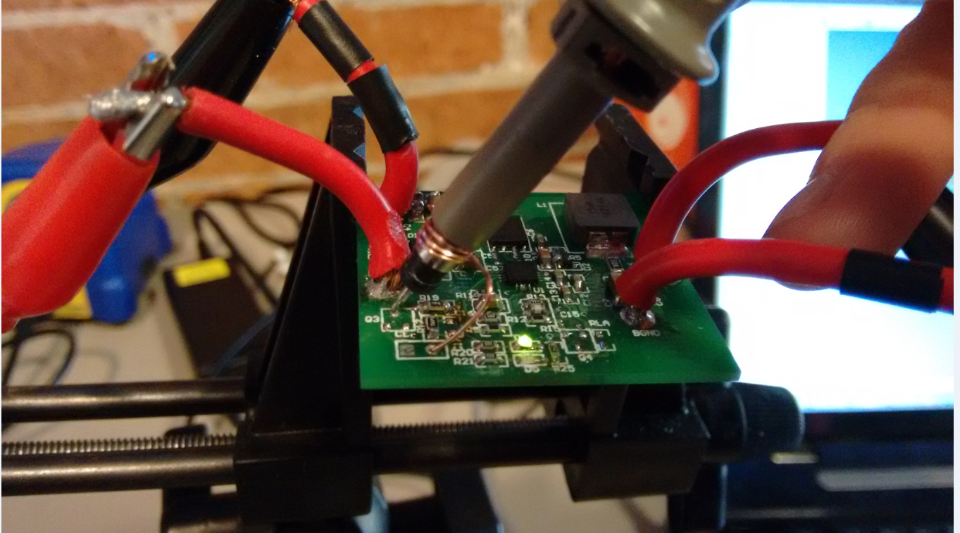
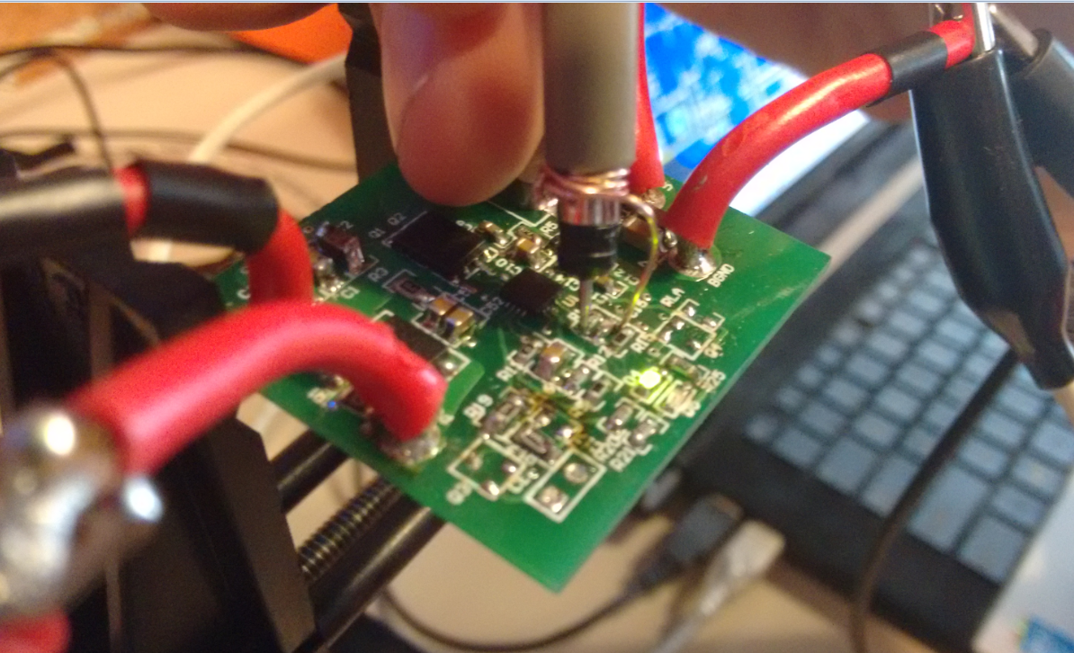
I have been playing with the BQ24650 circuit and made my own PCB and for truly understand the functionality I have came up with this questions.

For reference, I'm using a 12 Volt Lead Acid Battery with a charging current maximum of 1 A. I have used the application report for making the modification with another transistor and resistors for pulse charging

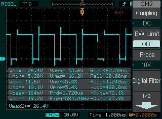
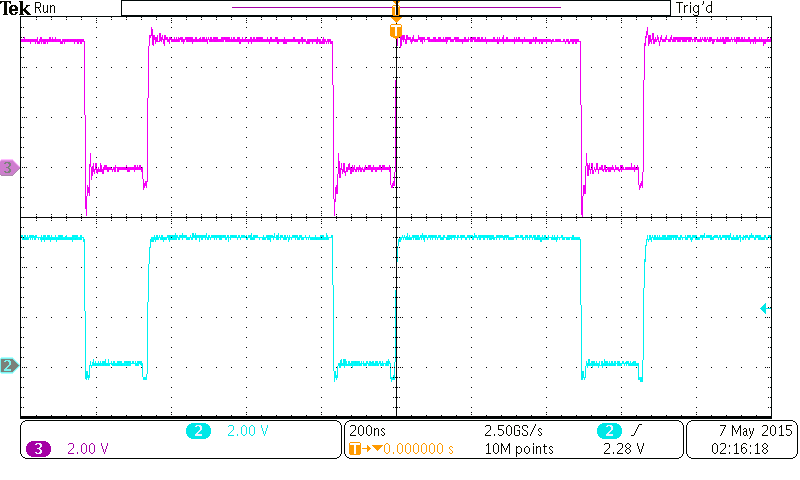
1.  In the application circuit of the eval board , D2 and R5 in junction with C6 creates a Boostrap circuit. Please clarify if correct and its properties 

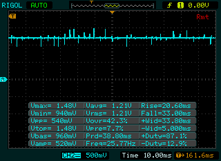
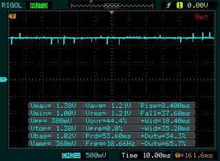
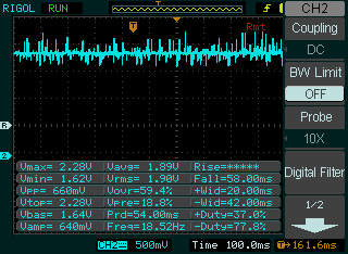
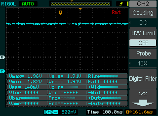
     1.1. How could I know ( by measuring) if the boostrap capacitor is being properly charge and discharged?

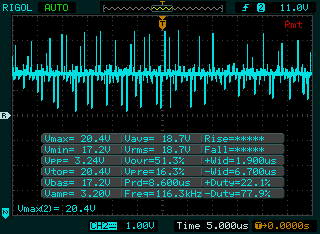
2. In the Eval board, C9 and R8 are designated for a snubber circuit, please clarify if correct. If its intended for a snubber can you recommend the values of the components, thanks.

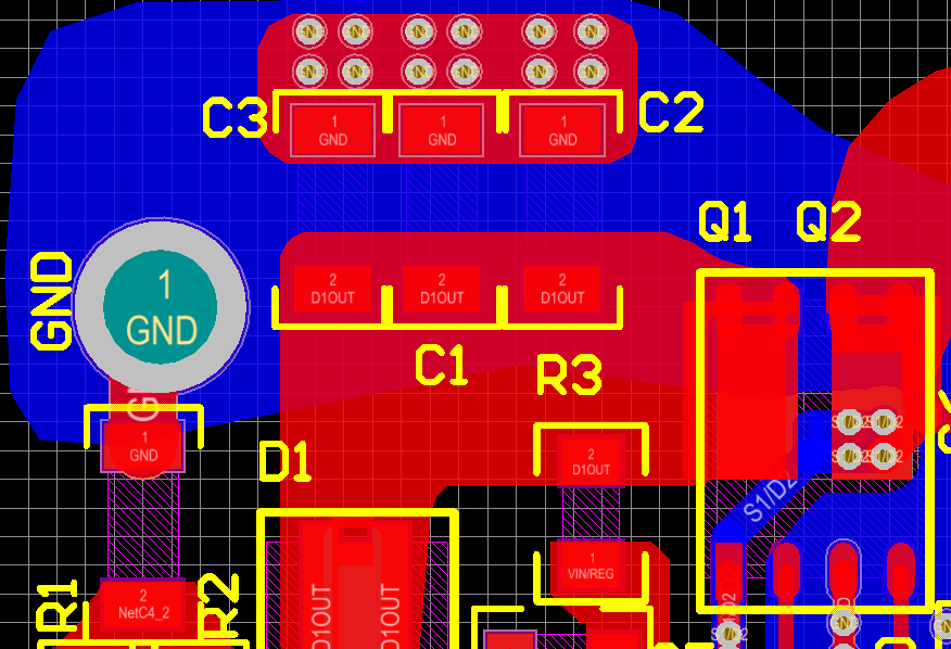
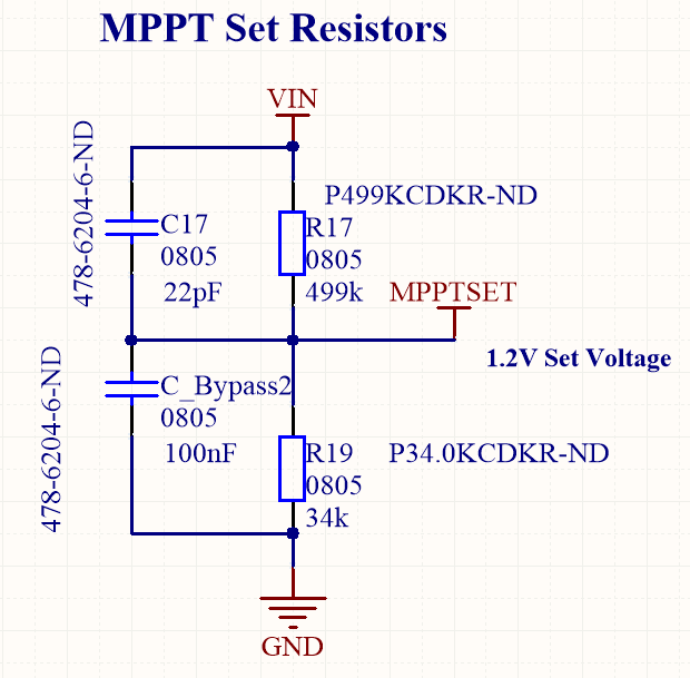
3. In the Eval board circuit, what is the purpose of C2 C3 and C1 ? How can I use them to improve a functionality of my circuit? Are the values from the eval board a good reference value or can they be improved?

4. For the output capacitor's labeled as C7 and C8, should we considered the DC bias characteristic of the capacitor to calculate the effective capacitance? Will this corrected value improve my efficiency? 

5. I think is already solved but can you please re affirm if I can remove the input diode D1 knowing the risk of reverse polarity ? Or does it takes part of the input filter? 

6. Im not using the Vsys Diode (D3) so I removed it. Was this a good practice or should I leave it ? 

Thanks for your help Geniuses ! 

    1. D2 and C6 form the bootstrap circuit. R5 is not necessary. It's purpose in the circuit is to slow down the rise time of the HIDRV, and the value of this resistor is heavily dependent upon the FET chosen and layout. It's good practice to put in a placeholder (zero Ohm resistor) so that you have pads on your PCB to tweak the rise time of the HIDRV during evaluation.
      1. You can use a differential probe and measure the voltage across C6. It shouldn't discharge too far below 4.2V (the IC will try to re-charge the cap when the voltage across C6 is less than 4.2V for three consecutive switching cycles).
    2. The purpose of a snubber circuit is to dampen the ringingyou see on the PH node. The ringing is dependent upon your layout and external components and could vary to from design to design. The snubber values needed for your design would need to be determined based on the ringing on the PH node of your PCB. A snubber circuit will also lower your converter efficiency.
    3. C1 is the de-coupling capacitor for the downstream circuitry on the VSYS node. C2 and C3 serve as the input capacitors for the switching converter. The final values of C2 and C3 is heavily dependent upon your PCB layout. However, the values in the EVM is a good place to start.
    4. Yes, use the DC values for those capacitors. Keep in mind that once a voltage is applied on the ceramic capacitor, it's value could reduce by ~10-20%. Refer to the capacitor manufacturer's datasheet for this. If you are charging a 12V battery, make sure your voltage rating for the capacitor is at least 16V (25V is even better, but that could result in a larger dimension capacitor).
    5. D1 is also a blocking diode when VIN < VBAT. This ensures that the battery does not discharge into VIN. It also serves as part of the input filter to ensure that during a hotplug of VIN (which could cause ringing on VIN), the battery doesn't discharge into VIN. It is recommended that D1 is left in the design unless you are sure that your VIN power supply cannot sink current from the battery.
    6. D3 serves as a more efficient path for current to flow from the battery to VCC of the bq24650. Removing it will force current to flow through R6, L1, and Q1:A to reach VCC - which is far less efficient. If you are OK with the power loss of R6, L1, and Q1:A, then you could leave it off.

  • Hi Smriti , This information will help me a lot in my design. 

    In the last questions I just want to make clear this

    1. I have in my design a 2 ohm resistor as suggest in the EVM. I will still check the rise time of the Hi Driver to see if it has the correct value.

    2. Ok, understood the snubber

    3. Ok, understood

         3.1. For C1 y used http://www.digikey.com/product-detail/en/0/1276-3190-1-ND

         3.2. For C2 and C3 y used www.digikey.com/.../1276-2789-1-ND

         Any comments ? 

    4. Ok, understood, I think it will be worth to mention it in the datasheet, Dont you think?

    5. Ok, understood

    6. When you say "Far less efficiente" will the cost of the diode justify this power loss on L1 R6 and Q1:A?

    The main reason of all this questions was to solve my noise problem. 

    Let me attach some images:

    This is my PH node. DC coupled with 0 DC offset

    This is my PH node AC coupled 

    This is my VIN Pin (Righ now comming from a lab DC source) Viewed with -17Volts DC offset

    And finally, this is my PCB layout for my input capacitors 


    Due the noise I though of placing a snubber. 

    I have been playing with input capacitors to reduce the input noise but haven't come up with any good results

    Do you have any recommendations to improve my design? Righ now the system is charging the battery, but of course, for a stable design this noise has to be eliminated. 

    Very thankful for you help

    Hope to talk you soon 

    Kindly

  • #3. Looks fine. Are both C2 and C3 going to be 0.68uF? I would recommend other higher values (like 1uF and 4.7uF) in addition to 0.68uF.

    #4. It is listed in the datasheet. Page 21, the paragraph right under equation #13.

    #6. That's something you will have to decide for yourself. Trade off between battery life in standby/sleep vs. cost/size.

    I think your overall problem may be your measurement method. Are you using proper scope probe placement methods (like tip and barrel, or using scope probe test points as used on the EVM like TP2)? Do not use the ground lead on your scope probe for these measurements because the loop that is created with the scope probe ground lead will pick up the the emitted radiation from the SMPS. See the following app note (figure 6 in the app note) for the tip and barrel method: 

    The following scope capture shows the same signal capture using the scope ground wire (CH3) and using the scope probe test point like TP2 (CH2). You can see a big difference in noise.

    It's hard to tell from your layout if the placement of input capacitors is ideal. It's not just the placement of the input capacitors, but how small the AC loop is to keep your noise at a minimum. Make sure you are following ALL the guidelines listed on page 25.

  •  

    Thanks Smitiri for your quick feedback and rich answers


    For the numbers


    #3. Recommendation taken, thanks. Will still check the bias effect


    #4. Yes you are right.


    #6. I really don't see how this diode (D3 PDS1040) will improve my battery life. Can you specify please?


    I'm using the probe test that my humble Rigol DS1052E provides

    The TP2 tip right now is far from my hands unfortunately to implement it on my already fabricated PCB. Will include in the ver3

    Its curios because I have the EVM and have tested the same points from where I'm getting noise.

    And the signals in the EVM look clean even though I did used the GND clamp in junction with the probe (Contradicting your suggestion)

    Still, by the facts that you mention I might be measuring wrong. What other methods can I use to test the TRUE signal?


    I have created a link that has all my signals. Please take a look at the plots.

    I used the GND clamp for reference.


    www.dropbox.com/.../AAAGFusr228uHAvH_vaNUhASa


    With the last reply I have come up with several questions regarding the BQ24650 #2 which I list below from number 10:


    #10 If you see the plots, HIDRV voltage is Higher that LODR considerably. Are the levels of the drivers correct? I can see the Datasheet plots on page 8, just want to make sure


    #11 Right now I have a Lab supply acting as the "Solar panel". I limit the current with a max output of 300mA. But if I raise the current to the current which the sense resistor is programmed (1A), when reaching approx. 500mA the MPPT stops regulating but is still charging but at approx. 250mA. I think is due the noise that gets higher. Can we discuss a possible problem due this behavior?


    #12 Im using this capacitor as feed-fordward cap: www.digikey.com/.../478-6204-1-ND. Both MPPT and VFB. In the MPPT pin, if placed, the noise get higher than without the cap. I think it’s also related to the noise. Do you have a comment on the selected cap and the behavior?


    #13 I asked about the DC bias of the output cap. So it will be the same story with the Input cap right?


    #14 Does TI provides a private channel with your person in which I can share my PCB and design for a quick review?


  • #6. The voltage drop through R6, L1, and Q1:A will be greater than the voltage drop through D3. So when you are in sleep mode (when input is not present), the IC is powered from the battery. Greater voltage drop = greater power loss = lower efficiency.

    The amount of noise you pick up through your scope probe ground is also heavily dependent upon layout. The EVM layout is optimized (by keeping the AC loop as small as possible) which is why it doesn't generate as much EMI as your own layout might. You can also get a short ground lead by wrapping a metal wire against the metal exposed ground of the scope probe (see the following image): www.cliftonlaboratories.com/.../Update202.jpg. Retry taking the plots again with this method to see if the measurement gets any better.

    Also, make sure you are properly using analog ground and power ground as shown on the datasheet (figure 1) and EVM. Tying everything to power ground will cause noise to be injected from the SMPS to small signal pins like TS, MPPSET, and VFB, thus causing the charger to behave erratically.

    #10. Yes, that's correct. To turn on a N-channel MOSFET, gate needs to be higher than the source. Since LODRV is driving a low-side MOSFET (with source tied to GND), you only need 6V to fully turn on the MOSFET. But on the high-side MOSFET, since source is PH node, and PH node toggles goes to VIN when the high-side MOSFET is conducting, it needs to be 6V above VIN to be fully on. In your case, that happens to be ~25V.

    #11. This is probably because as your raise the current, there is more noise on MPPSET. This will change the DC point on MPPSET. Trying placing a decoupling cap on MPPSET (maybe a 100nF cap?) to see if it gets better. You will have to play around with this value.

    #12. This does not make sense to me. With the cap on MPPSET, there should be less noise (and noise should decrease with more capacitance). Could you attached a scope shot of the pins with and without the cap? Also, make sure the cap isn't too large on VFB, as this will affect your transient loop response of the SMPS.

    #13. Yes, that is correct.

    #14. I will send a private message to you through this forum. Please respond to that with your schematic and gerbers.
  • Dear Smitri 

    #6. Ok, thanks for the explanation

    Regarding the measuring method, I had taken this shots and you are right. Having a small ground wire reduces significantly the noise

    MPPT pin with normal measure technique. Long ground cable

    MPPT pin with short ground wire

    VFB with normal measurement technique 

    VFB with short ground wire

    One point to view is that the VFB pin had the 22pF cap and the MPPT pin dont.

    This is how I measure the different pin

    Measure on MPPT pin

    Measure on VFB pin 

    Tip configuration 

    Regarding the ground, I did make the separation from the analog and power ground and join them in PAD as the datasheet suggested

    #10, Ok, thanks for the explanation

    #11. Ok, Will do that. I will try adding this configuration for my next iteration. Both MPPT and VFB pins. Will you have a comment on this 2 capacitor / filter array?

    Take a look of my proposal 

    For MPPT

    For VFB

    #12. Above are the scopes of the pins. I think was probably because of the measurement methods. When you say the capacitor on VFB, you mean the 22pF in junction wiith the battery node? Thanks

    #14. Information already sent.

    Just another question

    #20 , My tests were made charging several 12 volt 12 Ah batteries. As I stated in the last comments, if I increase the current, the charge controller will stop regulating and the MPPT option was turned off. This will happen if my charge current is above 400mA. I tried charging a 75Ah battery and encounter the same problem but the max current from which the charge controller will stop MPPT regulating was 250mA. Lower than the 12 Ah. So we can determine that the main problem is the noise in the lines. Im I correct?

    I have created another PCB with the recommendations and suggestion you have made ( Return of D3, bypass caps) I want to wait to see if you detect an error in the PCB that I send you.

    Thanks for your rich information.