This thread has been locked.

If you have a related question, please click the "Ask a related question" button in the top right corner. The newly created question will be automatically linked to this question.

TPS63011 UVLO

Other Parts Discussed in Thread: TPS63011, BQ25505, TPS63036, TPS63050

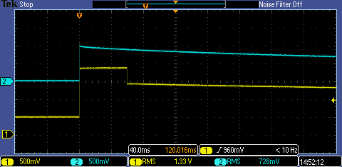
I'm using a TPS63011 in a circuit which is fed from the output of a BQ25505. According to the spec the UVLO should be 1.5V min, 1.8V max yet with an input of ~1V I'm seeing ~400mV on the output. Shouldn't the regulator be effectively off until an input voltage 1.5V and the output be 0V?

  • We don't see this on the EVM. Could you post your schematic and a waveform of Vin, Vout, L1, and L2?

    As well, the TPS63011 is a higher power buck boost. I'm not sure you need such a device for a harvesting system. What power specs does it meet in your system?
  • I sent you a PM with the schematic and I'll post scope plots later. TPS63011 is a little overkill but we liked the low Vin and wanted to leave headroom on a circuit that can draw up to 300mA . We also wanted to use the Vsel function to help lower the overall power when in sleep mode.
  • Thanks for sending. We have the TPS63036 which is way smaller and does down to 1.8Vin. As well, the TPS63050 is most efficient but only goes down to 2.5Vin.

    I'll look at the waveforms when you post them.
  • OK, I know I made a post last week with the scope plots but coming back I don't see my reply. I don't remember all that I said (yes, I'm getting old) but the BQ25505 was/is putting out a higher than expected voltage for a short period which was just long eough to turn the TPS63011 on briefly.

    Here's a zoomed in shot or the trigger

    And here's a shot showing the BQ25505 cycling (during MPPT checks every 16 seconds):

  • Yes, it seems that you do not have a stable and sufficient Vin. So, I expect that your DMM is averaging these waveforms and giving you 1V on the input and 400 mV on the output, when in fact they are changing signals.
  • Now for a separate question that I've just run across which has me a bit puzzled. My initial testing was with the VSEL pin pulled low (through a 10k) which sets the part for 2.8V output. With this setting I was able to run some tests with small solar panels and no load connected and with relatively little output from the solar panel the circuits would work and the TPS63011 would create the 2.8V rail.

    I wanted to see how the system worked with 3.3V output from the TPS63011 and I tried changing VSEL to a 10k pull-up to Vin. The BQ25505 was not able to charge up enough to create the battery charging voltage to 4.2V. I also tried directly tying VSEL to VIN but I got the same results. Looking at the efficiency curves I don't see much of a difference whether the TPS63011 is outputting 2.8V or 3.3V but from my testing the solar panel needs to be supplying a lot more power in order for the BQ25505 to generate the 4.2V battery charging level which then allows the TPS63011 to generate the 3.3V output.

    Nothing in the circuit changed except for the VSEL pin yet the operation of the circuit is vastly different. With VSEL low I was able to get the circuit to work indoors yet with VSEL high the circuit ONLY works in full sun. Since the output of the BQ25505 is feeding the input of the TPS63011 I figure somehow the TPS63011 must be presenting more of a load yet I don't see that in the datasheet.

    Can you shed some light (yes, pun intended) on why I'm seeing this behavior?
  • 3.3Vout requires more charge to be pumped into the output caps. This is more energy.

    To get these types of systems working optimally, you need to look at waveforms of good and bad cases. Delaying the startup of the TPS63011 is one method frequently used to allow the bq device to deliver enough energy in storage capacitors to achieve startup.

    Keeping loads off until the 2.8V/3.3V rail is on is another way at reducing the current required to startup.

    The TPS63050 has an adjustable SS time and input current limit which can help in these types of power limited systems.
  • That's true, and I would expect some additional power needed but the change was so drastic it threw me off. It's hard working on this design since the workbench has no sunlight I guess I'll have to mobilize the scope and start taking a closer look at what is going on.

    Yes, I've used the TPS63050 in other designs and did use the SS to delay the turn on of the regulator. Unfortunately that part only goes down to 2.5V so it's not an option. I guess I could add a cap on the EN pin of the TPS63011 which would delay the turn on some but then the BQ25505 would have an additional load charging that cap (albeit a small value) so I might be fighting myself.

    What's your thoughts of eliminating the 10uF input cap (C9) of the TPS63011? The power source will ultimately be coming from a Li-ion or alkaline backup and there's also the 1uF on the output of the ORing circuit that selects between the 2 batteries.
  • Hi George,

    can you please post a schematic and a photo of your test setup?

    You need the C9 input capacitor to reduce the input impedance. Without that, the converter's input voltage might drop too much during switching, which could lead to instability.
  • Chris has the schematic so check with him please. I wasn't suggesting running the TPS63011 without any input capacitance but here's a snippet of the design:

    C9 and C15 are placed right next to each. The power source will either be a Li-ion or alkaline batteries so there's plenty of capacitance from those sources which are also placed quite close to the input of the TPS63011.

    I don't typically remove input capacitors when when circuits are daisy chained together like this and I'm having issues I start to look for creative ways to improve the circuit.