This thread has been locked.

If you have a related question, please click the "Ask a related question" button in the top right corner. The newly created question will be automatically linked to this question.

LP3981ILD thermal dissipation problem

Other Parts Discussed in Thread: LP3981

I'm using the LP3981ILD in VSSOP, The Vin=5V Vout=3.3V I=250mA for the 0.4Watt power. The case reach 100° too much. I have a 10mmx10mm copper area bottom side with 4 vias.  Is there a layout raccomandation to joint RjA = 56°/Watt with copper area  ?

Thank you

Michele Mazzacchi

  • ..”Is there a layout recommendation to joint ΘRJA= 56°/Watt with copper area  ?”

    The ΘRJA = 56 is for the WSON package, the ΘRJA of VSSOP is 177; the WSON package has better thermal resistance than the VSSOP package due to the exposed thermal pad.

    The ΘRJA spec in the datasheet is calculated using a JEDEC_51-7 standard test board, this spec its best used as a comparison between packages thermal performance instead of system/application board thermal performance. The ΘRJA is directly related and influenced by cooper area and layout. Increasing the cooper area will greatly improve the thermal performance.

    To better approximate the junction temperature of the IC in your application board is recommended to use  Ψjt or Ψbt thermal parameters instead of ΘRJA.

    Please take a look at SPRA953B and SBVA025 . these appnotes explain the thermal metrics and how to improve the thermal performance.

    Best regards,

    Antony Pierre

  • Thank you very muche for the answer, i had seen the SPRA953B,  but i don't understand how muche is the layout PCB copper for the jedec-51-7. It recommend Board Finish Thickness 1.60 mm ± 10% Board Dimension (pkg length < 27 mm) 76.2 mm x 114.3 mm Board Dimension (27 mm ≤ pkg length ≤ 48 mm) 101.6 mm x 114.3 mm Board material FR-4 Trace Copper Thickness 0.070 mm ± 20% Trace Width, Finished 0.25 mm ± 10% for ≥ 0.50 mm pin pitch Lead width for < 0.50 mm pin pitch Trace Coverage Area (Total) Power/Ground Thickness 35 µm (1oz) copper +0/-20%.  I don't find the trace coverage area data, do you know it? Your sincerely  Michele Mazzacchi

  • Michele,

    The pin pitch and package description is in the last section of the datasheet. The pitch of the DGK (VSSOP) package is 0.65mm so the trace width shall be 0.25 +/-10% for the JEDEC51-7 board.


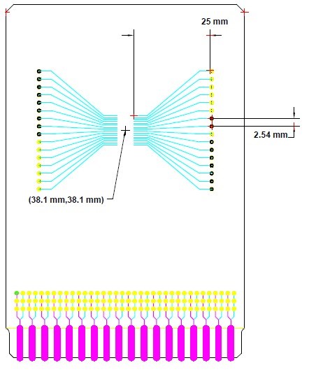
    To add to your JEDEC51-7 description: the board does not have cooper pour on the top layer and bottom layers, in the top layer there is only the traces connected to the package and must extend at least 25mm out from the edge of the device body.


    The picture below shows an example of a generic JEDEC board layout


    In the case for the LP3981 the JEDEC board will only have 4 traces ~10mils width at each side of the package, that is not much for thermal relieve. A better layout example is in page 15 of the datasheet, the example is for WSON package, but the dog bone layout concept applies for the VSSOP package as well.


    Best regards,

    AC

  • Thank you very much, now i have clarified my doubt regards the jedec51-7.

    Your sincerely

    Michele Mazzacchi

  • " ... I'm using the LP3981ILD in VSSOP ... "

    I'm confused on which package this is about:  LP3981ILD = WSON, or LP3981IMM = VSSOP

    Using : Tj = (Ttop + (Ψjt × PD))

    For your application : PD= ((5.0V - 3.3V) x 0.25A) = 0.425W, and (presuming) Ttop = Tcase = 100°C

    For LP3981IMM (VSSOP) : Ψjt = 10.8°C/W.

    Then : Tj = (100°C + (10.8°C/W x 0.425W)) = 104.6°C

    Yes, that's warm, but still within the LP3981 operating junction temperature range.