This thread has been locked.

If you have a related question, please click the "Ask a related question" button in the top right corner. The newly created question will be automatically linked to this question.

My problem with TPS61088

Other Parts Discussed in Thread: TPS61088

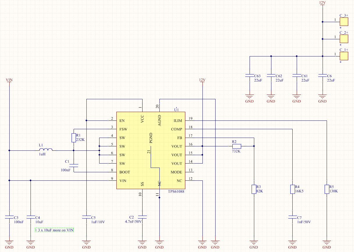
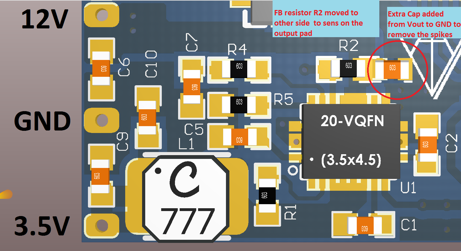
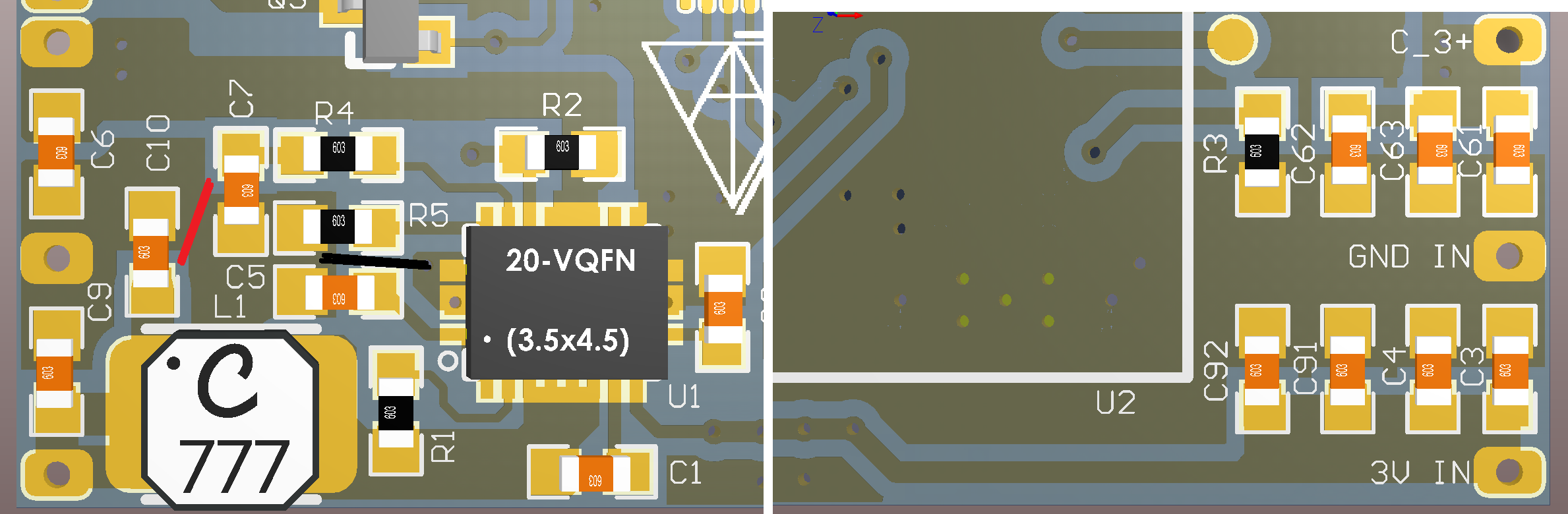
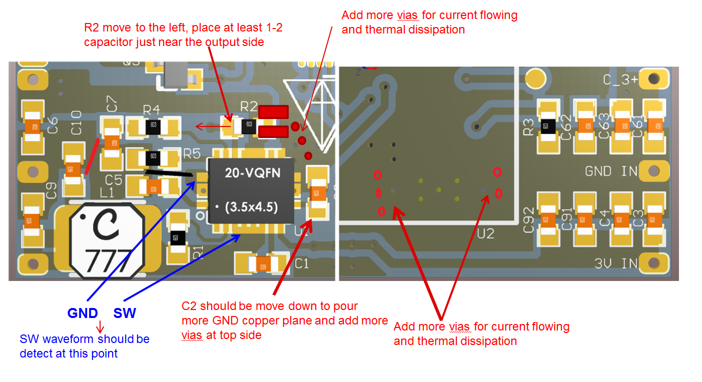
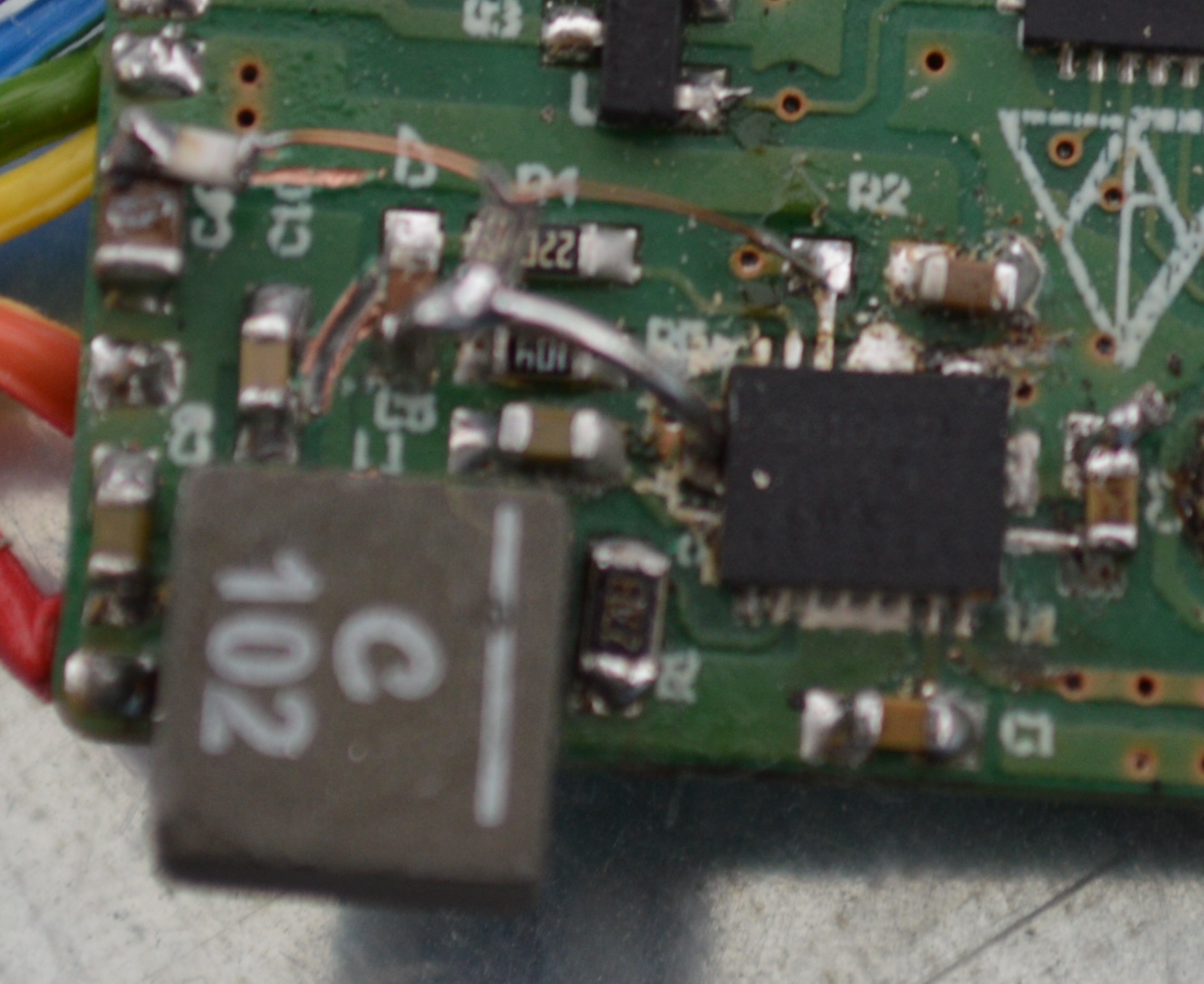
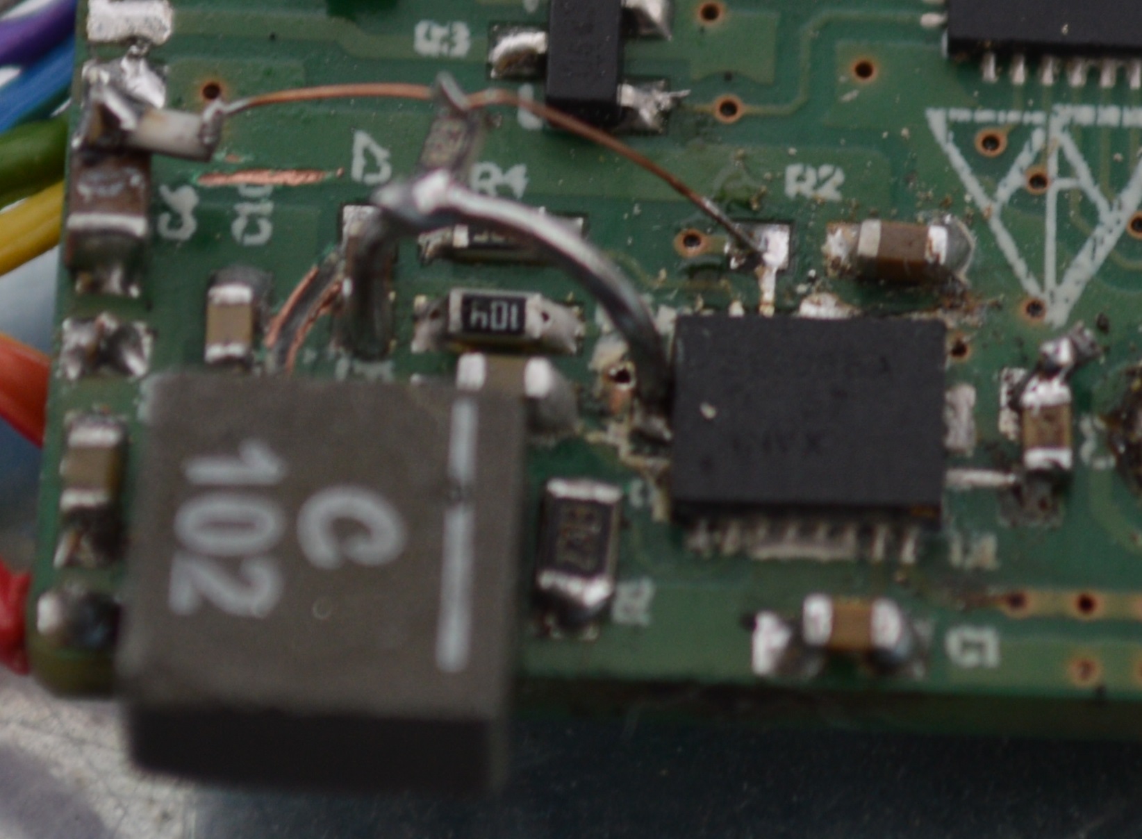
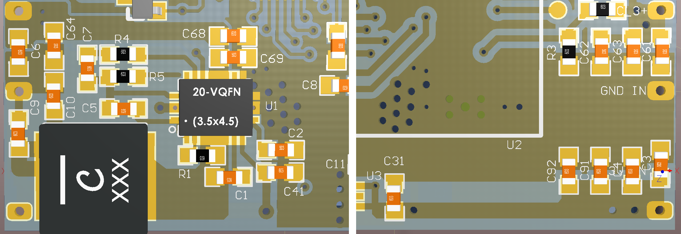
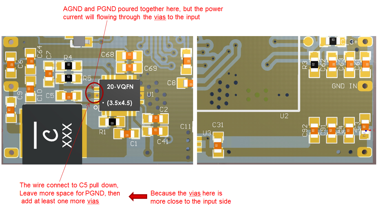
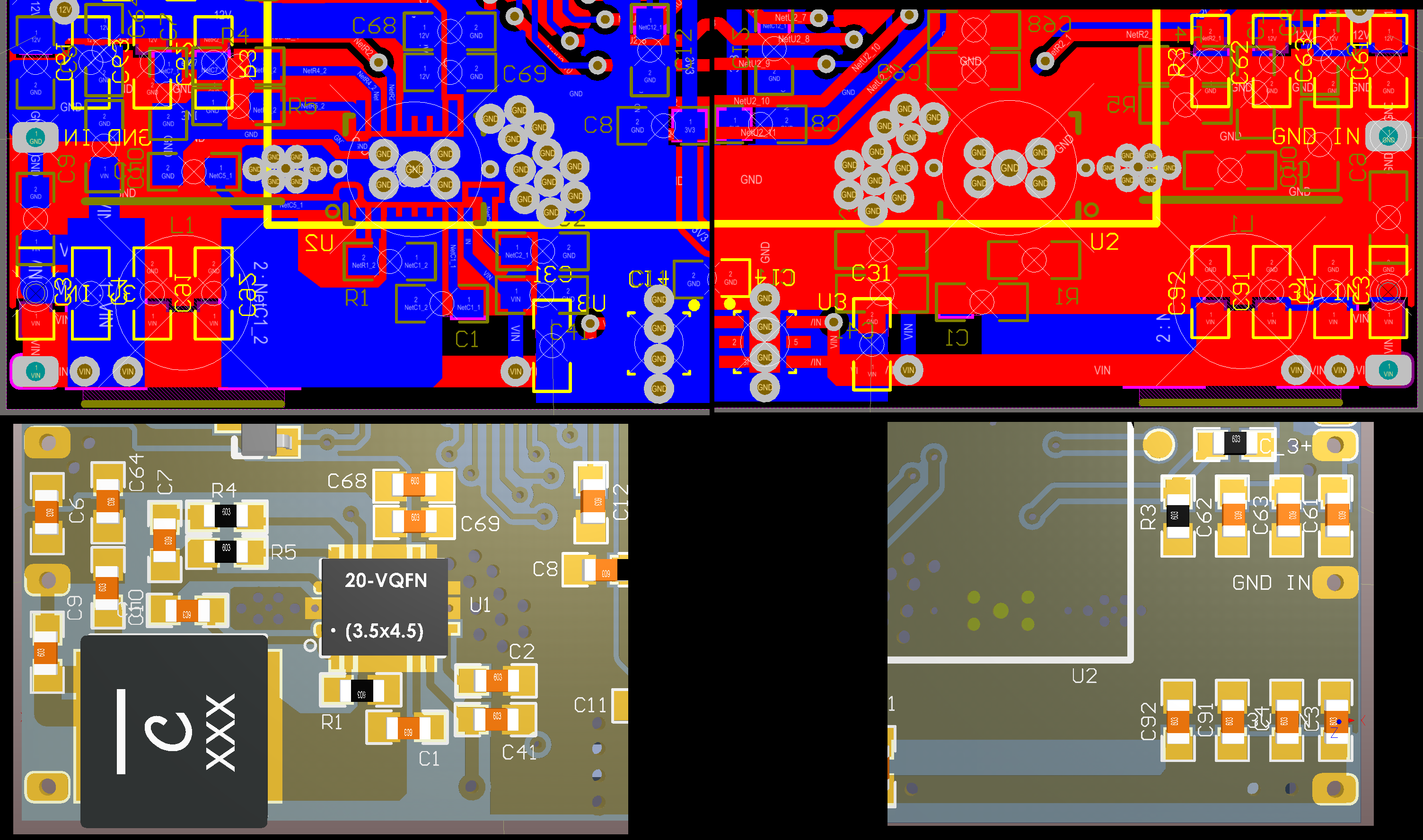
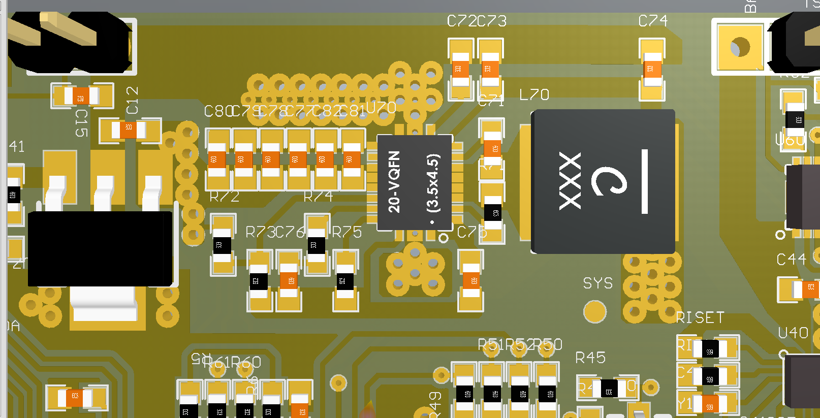
I have the below schematics. I need on output 12V 0.6A, but let say 1A to be on safe. I built it and first tried with XAL4020 1uH. It has the 12V on output, but once increase load it drops, and IC burns. I have bought the developer board and that works fine. Changed the inductor to XAL6030, it increased the loadable current, but still burns some ICs. Changed the inductor with that one from dev. board, seams to be better but still kills the IC at higher loads. Once the IC is damaged than the IC and inductor get hot, and load high current from source, but still try to work.

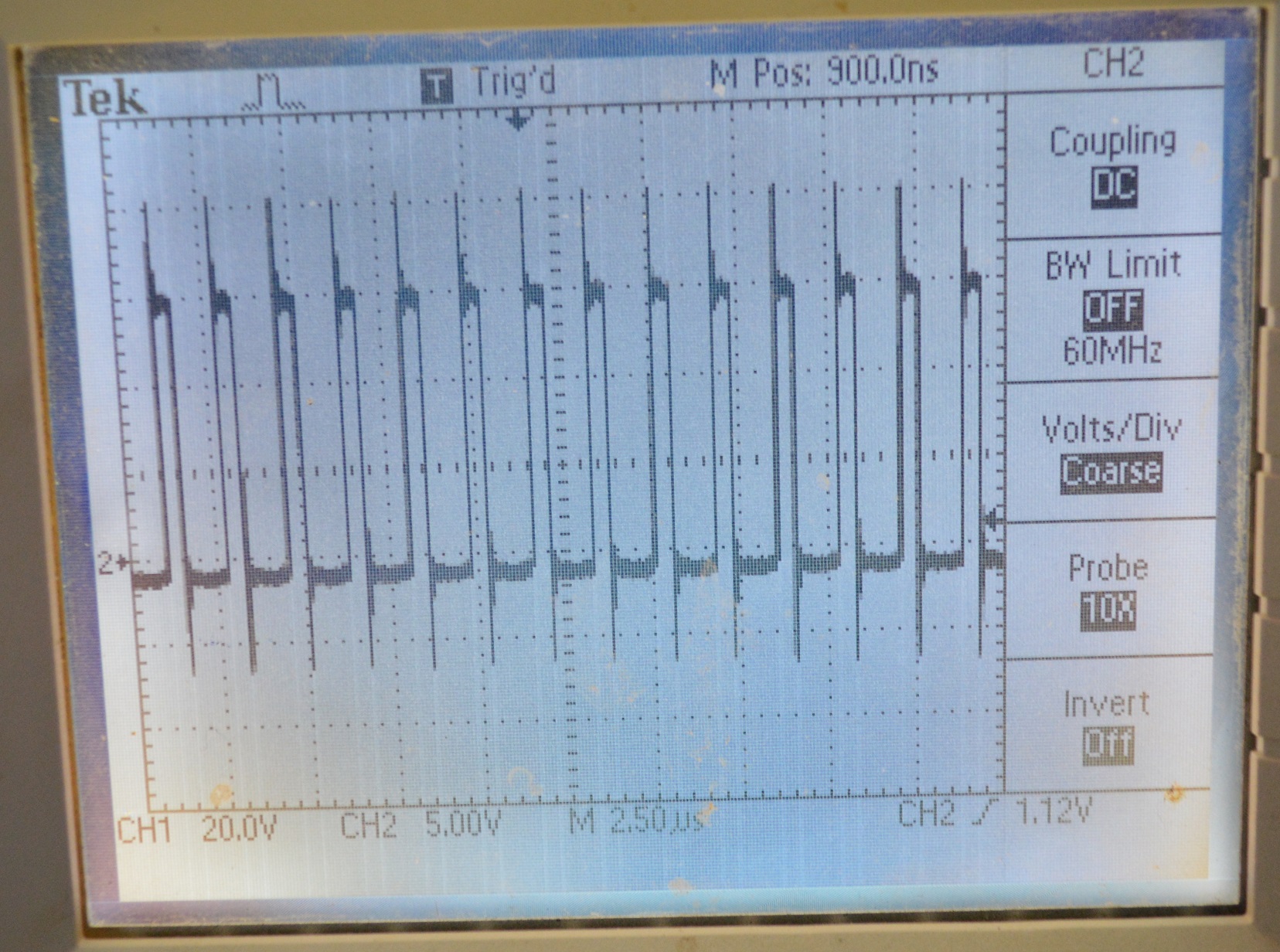
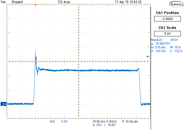
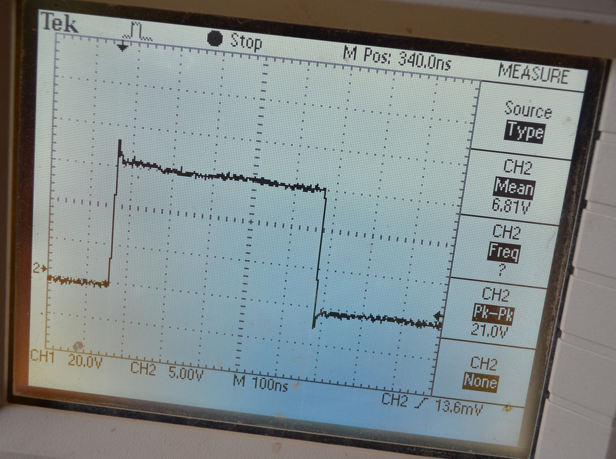
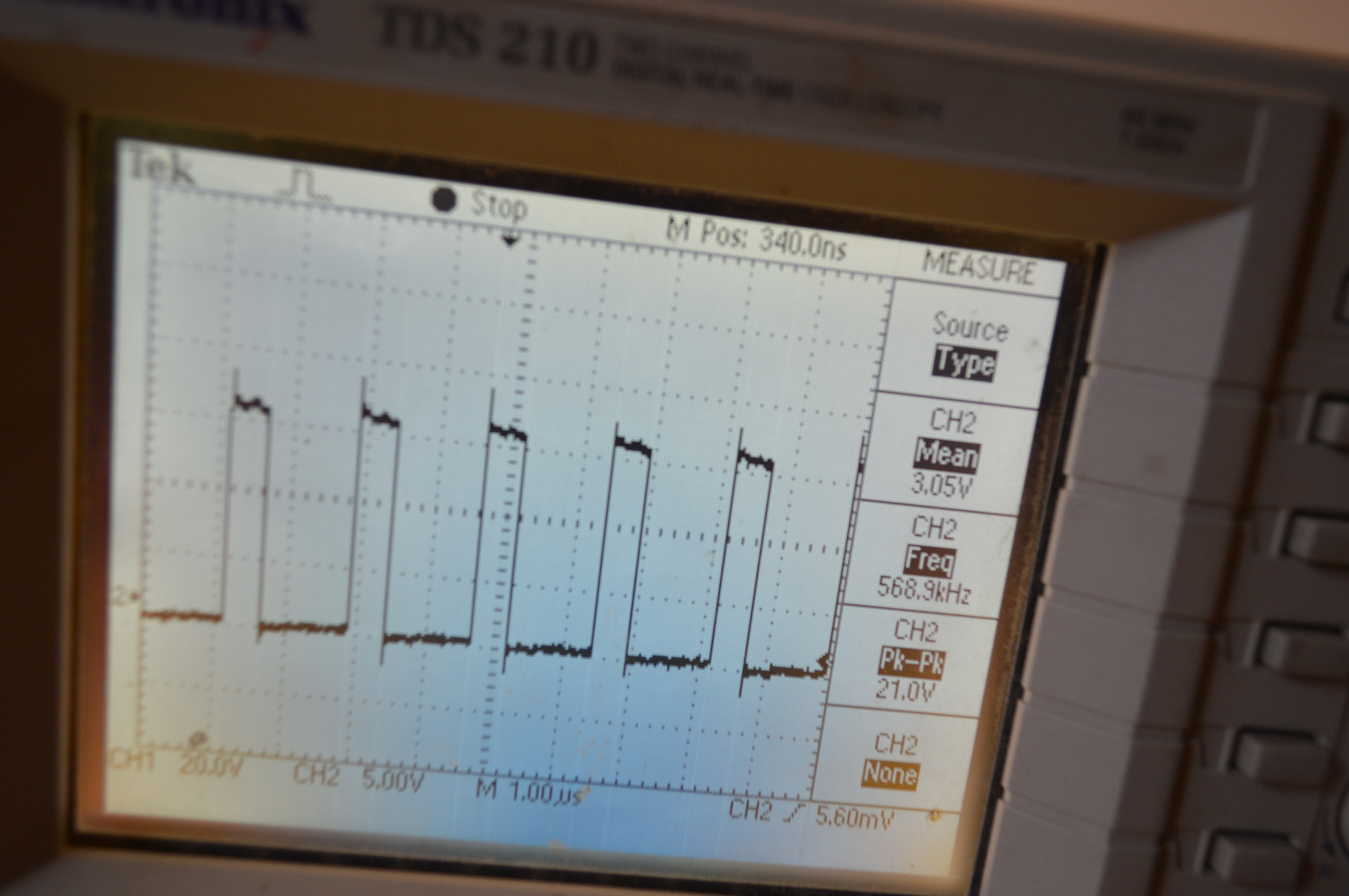
Looked at SW pin and it looks that my electronics has higher spikes than the developer board, that may kill the IC ?

Has anyone idea what Im doing wrong ? I burned already over 10 ICs, during trials.

Thank You so much !

Zoltan

  • Removed the inductor from the developer board and added my 1uH XAL6030 inductor and it works fine with 15W load, so the inductor cant be an issue.
    Removed all in and out capacitors from the developer board and added just 1-1 of mine to in and out. The developer board still work.
    Checked the SW pin on the developer board and mine looks same, same pk-pk at 25V with 3.5V input.

    My board has same 12V output as the developer board, but the inductor temp is sensed by hand (not hot) even is no load on its output. While the developer board inductor with no load is cool.

    I found some spikes on the Vout pin, added a 1uF just to the pin and it dissapaired. The 12V were clean at output capacitors.

    Checked that is no drops on power and ground traces.

    Has anyone idea ?
    Please help as the product should be already in production and this small issue lock me since 2 weaks.

    Thanks !
    Zoltan
  • Absolute maximum voltage on the SW pin is 14.5 V. Are your spikes exceeding that? Also, if your SW node spikes are too high you will need to look at the PCB layout... how does your PCB layout compare to the TI EVM? You could also consider an RC snubber from SW to GND.
  • Thank You John !

    The signal on SW looks exactly same on developer board than on my PCB.
    I have attached the PCB drawing.
    If You have any idea is very welcome !
    Thanks
    Zoltan
  • Today killed the developer board too. Developer board with below modifications:

    replaced 2 input C with one 0805 10uF/6.3V

    replaced 4 ouput C with one 0805 22uF/25V.

    removed output C of 1uF

    replaced inductor with 1uH XAL60


    The signal on single working unit (my pcb) on SW pin is like below. May be the spikes are the main problem ????

    And signal on SW with DC coupling. It looks that the voltage on SW is on edge. Do You recommend something ?

  • There is definitely something not right with your circuit.  The SW node should roughly switch between Vout and GND.  For a 3.5 Vin to 12 Vout, the duty cycle should be about D = 1 - Vin/Vout = 70.8%.

    Your SW node is operating at around 30 % Duty cycle and the output appears to be closer to 14 V.  If I calculate correctly, R1 = 232k = 2092 kHs Fsw.  can you clarify your design parameters?

  • Yes 232K is the right value. You can see all other values on the schematic attached before.
    I have tried to lower the frequency by changing the resistor to 270K, but the signal looks same, regarding level.
    The Sw measurements were done without load.
    Its interesting that the developer board shows almost same signals, before died.
    The output has a several 22uFs on output, and it looks a clean 12V.
    The circuit works fine just can not be loaded as it die.
    Today I connected the developer board to a single cell li 18000mAh and it turns on the 12V, 15W LED on its output. I just had a little "bouncing" during connecting Vin wires and suddenly the IC die. Probably the removed caps caused that, but anyway till now were unkillable, but now got the illness from my circuits.
  • Dear Sir,

    I'll check your schematic and PCB in detail and reoly you within today!

    BR,Helen

  • Hi,

    1) I noticed that the control signal GND and the power signal GND is mixed together. That is : the compensation network R4 and C7, output voltage dividing network R2 and R3, current limit resistor R5 should be connected to the control GND instead of the power GND.

    2) Another key point, which may leads to the failure of the IC is the thermal: the TPS61088 dissipate the heat through the bottom side thermal pad PGND. So you must leave enough space for the PGND for the thermal dissipation. From your layout it seems that the PGND area is not enough. And when the total power is higher than a certain value, the IC may broken.

    BR, Helen

  • I noticed that your SW waveform is abnormal, it seems that the output voltage is higher than 12V, looks around 14V. And the SW wavrform should be a≥0 waveform(like the waveform in the below), why the negative waveform in your test is so high? Did you measure it in the right way?

  • Right SW Waveform:

  • Dear Helen,

    Thank You very much for You overview. It is very appreciated as Im close to give up and look for other solution as my customer would like to have in production the product and I can not solve it. You are always asking about product qty., so I can tell You so much as I have signed an NDA, but the step up will be used to power 3 12V (total 600mA)LED strings from a Li battery. The production, were scheduled for beginning this year, so once this issue is solved would start asap. First batch is planed as 3K pcs for a trial than another 50K pcs is already scheduled for this year. As it is a new product, I dont see yet future plans of my customer.
    I have already designed this IC into another PCB were need to power 5V 2.5A from a Li battery, works like a powerbank. That project is to power and Ipad, to collect some sensors data on field. This is planed to be in production from March, but still affraid to order the protos, as I see some risk with TPS61088 usage. I have used quite a lot of TI ICs on recommended circuite, but never faced any issue.

    Please find attached both side of the PCB. As You can see the other side of the pcb is a big GND plane, could it be enough for cooling ? Anyway I didnt see any heating of the IC just burns suddenly.
    As GND separation I have marked 2 modification. A connection marked with black color and a pcb cutting marked with red color. In this way the AGN and PGND will be connected just under the IC. In this way the compensation network, divider, current limiter will be separeted to AGND. I will do this trial on my PCB, this should help ?

    SW signal - Strange that the output is a very clean 12V, in my circuit and developer board too- after I have changed the divider network and inductor. As prevention I have checked the SW signal - still it worked - on the developer board too and both looks same, just difference the pk-pk of dev board were 24-25V while my circuit were 27-28V. I will repair the dev board today and will take pic of both SW signals of dev board and my upgraded PCB.

    Thank You again for Your support !
    Zoltan

  • The output is a clean 12V, on both PCBs (dev board and mine) I have measured it.
    The SW signal were measured with oscilloscope GND connection at power supply side, so the wires may create the negative wave, even is to high to be just this. I have been surprised too, but let me some time and will do again after modification.
    Thank You for Your time.
  • Zoltan,

    Thanks for the detailed information, here's my feedback:
    1)  the step up will be used to power 3 12V (total 600mA)LED strings from a Li battery --> is that means the total output power is 3*12V*0.6A=21.6W? What is the burrn point? Around Po=15W?
    2) I see some risk with TPS61088 usage --> The TPS61088 is a very robust IC :) many customer use it, and till now we didn't found any issue, turst me :);
    3) As You can see the other side of the pcb is a big GND plane, could it be enough for cooling ? --> I noticed that all the current returned to the input side from the vias.  as the vias is very small , so please make the top side GND copper plane bigger and addd more vias on it.  Current vias and copper plane is not enough.  the vias outside the IC please use at least 20-24mil hole size .
    4) A connection marked with black color and a pcb cutting marked with red color. In this way the AGN and PGND will be connected just under the IC. --> good change. This will be helpful for the loop stability. but not helpful with the IC burn problem;
    5) the pk-pk of dev board were 24-25V while my circuit were 27-28V --> this spike is really too big. In our lab at Vin=3.3V, Vo=12V/2A output condition, the SW spike is around 20V peak. I think this is maybe caused by the detetion problem.
    6) I'll give output some suggestion on the layout in  the following picture.
    Good luck to you!
    BR Helen

  •  My suggestion on the layout:

  • Dear Chen

    Thank You so much for suggestions, I will do like that in nex revision. For now I have done some updates just by hand, in the air.

  • I have repaired both PCBs mine and ev. board to to have a comparison. The spikes looks that were due o long ground wire, so now I measured with ground

    near the IC.

    It looks that now the signal on my pcb are more friendly.

    The SW signals looks like

    The output signal without load (just one LED with 10K series) looks clean like

    Now I should add some load, but Im affraid a little based on bad experience. Could You let me know please that based on the signals it could be OK for now to test with load ?

  • 1) The final use will have 3 X 12V LED series, and the TOTAL current is 600mA, not each of them. But to be safe lets count with 1A at 12V. I have an LED string for test which is around 15-16W, that I use for testing.
    2) I have used a lot of TI ICs, and no one makes me so much headache. Im sure that this will work too at the end and I will gain some experience with it and QFN package replacing.
    3) I will update the PCB, thank You for suggestions.
    4) OH, than... Hopefully the updated signal pics will change Your opinion.
    5) Yes I found that the long GND wire to the oscilloscope cause that. Even with short 10cm wire there are but more smaller, and decrease a lot by shorting that with a metalic tweazer. So that probably cames from that.

    Thank You Hellen for all Your effort !
    Zoltan

  • Dear Hellen,

    Im updating the PCB, could You have a look please if it is OK in this way ?

    I have added bigger vias on the right of the IC. On the left there is no space as I have separeted the GNDs.

    Added caps close to the IC output.

    FB network moved on bottom side of the pcb.

    Added cap close to Vin and some more on Vout.

    At the moment I have connected the mode with GND, but as it is a battery powered device may be would be better to let it open,

    even we will never have less load than 50mA at its 12V output.

    During normal running the stepup output will drive the 12V 600mA LEDs with 10% pwm continuously, so we may count with 50-60mA load.

    Randomlly will change the pwm to 30, 60, 100% and back to 10% So will increase the load to aprox. 200, 400, 600mA. and than back to 50mA

    Which running mode do You recommend ?

    Thank You in advance !

    Zoltan

  • The version's layout is very good. But I can't see clearly where the PGND and AND connected together. The following is my comment.

  •  Dear Hellen,

    Thank You so much for support.  It is really welcome.

    The PGND and GND is connected just under the IC, this were a quite strong lesson to keep them well separeted. I have attached a 2D view to that may be more clear. Added some more vias too on left. Now the still open question is in which mode to run the circuit ? To connect the mode input fixed to GND or let it open ?

    Thank You for all Your effort !

    Zoltan

  • Zoltan,

    Right, AGND and PGND should be single point connected. This version's layout is very good. But the best single point connection place is to connect them at the AGND pin and PGND pin. Thus the PGND area can be bigger.  Good luck to you!

    BR, Helen

  • Dear Hellen,

    Thank You for all Your support. I hope it will works fine.

    I have already added into another project, were I had some more space. Hope that will perform well here too, but if You see any risk, please scream :)

    Thank You for all !

    Zoltan

  • Zoltan

    This version's layout is very good:)

    BR,

    Helen

  • Please click answered if you satisfied with the answer :)

    And could you please share your application information with us? Like in what kind of equipment? Volume? You can send the information to me by email, my email address is helen-chen@ti.com.

    Thanks