This thread has been locked.

If you have a related question, please click the "Ask a related question" button in the top right corner. The newly created question will be automatically linked to this question.

UCD9222+UCD7242 reports FLT

Expert 2985 points
Other Parts Discussed in Thread: UCD9222, UCD7242, TMS320C6670

Hi all,

My design is as follow

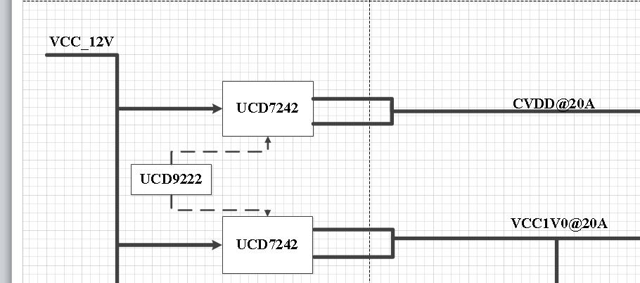
That is UCD9222's channel 1 controls the UCD7242's two channels using one identical PWM to generate CVDD that is 0.95V with 20A max current and the other UCD9222's channel controls the other UCD7242's two channels also to generate VCC1V0 that is 1.0V with 20A max output.

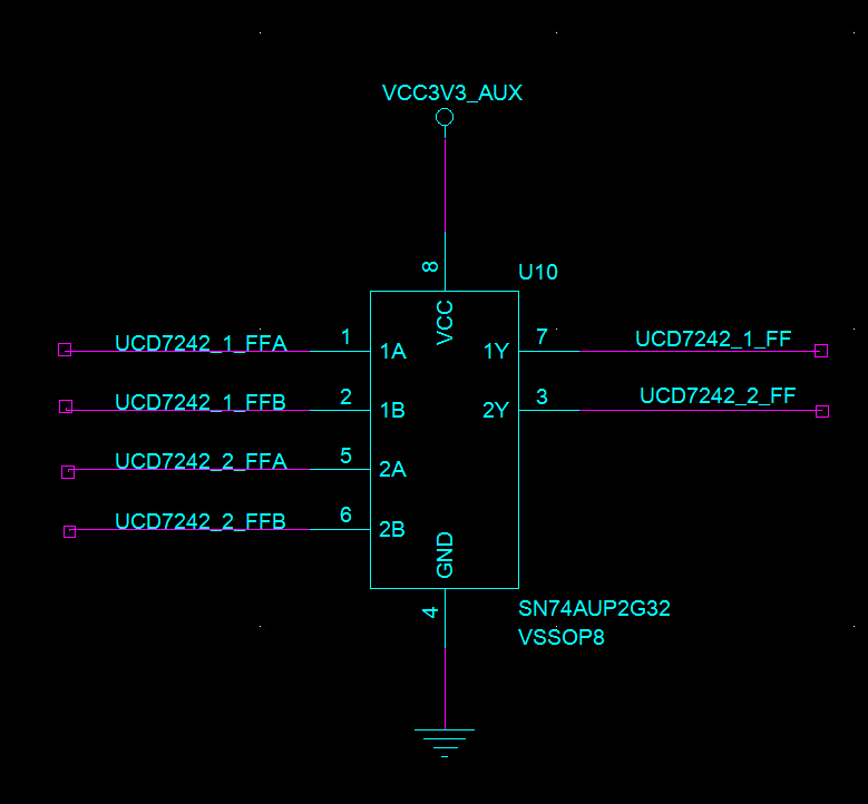
My schematics design is UCD9222_UCD7242.pdf

Actually, this power design is for one TMS320C6670.

Now I met a question that is VCC1V0 can be generated well but CVDD has no output and the UCD7242 that generates the CVDD reports FLT to UCD9222.

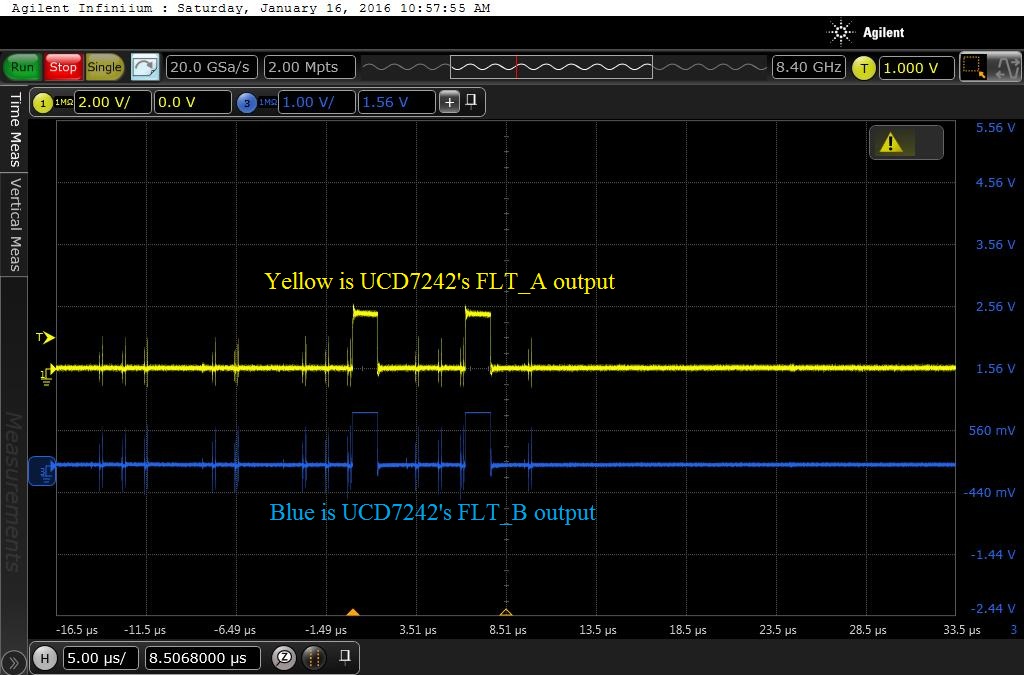
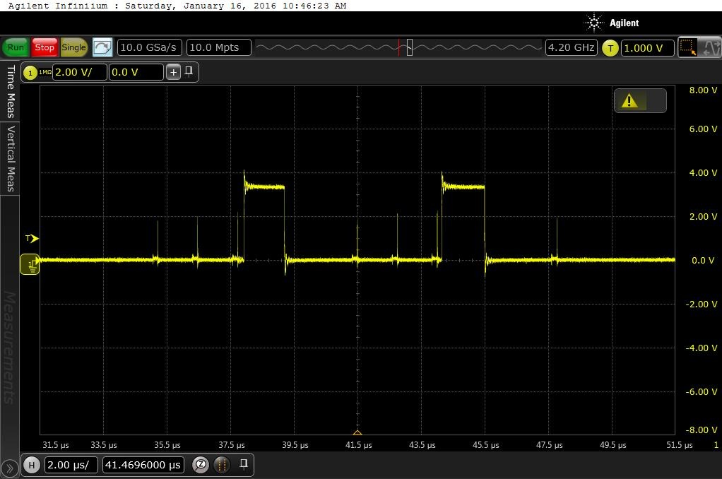
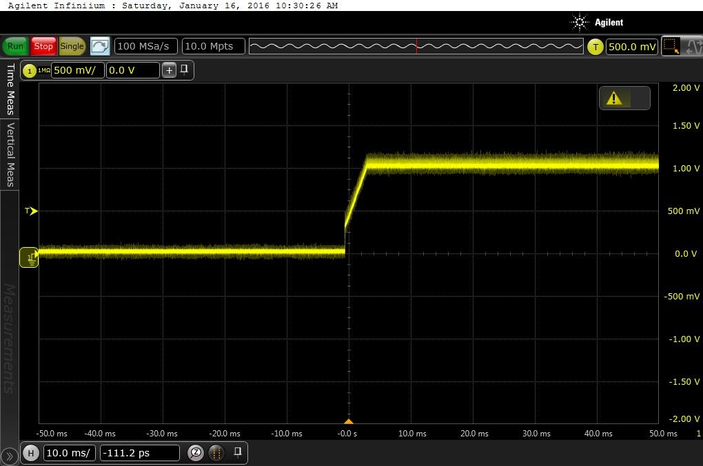
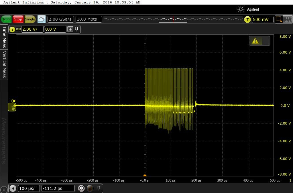
The FLT signal generated by UCD7242 is as follow. It is captured by oscilloscope.

My questions are

1. Why FLT signal is lower than 3.3V? Does this UCD7242 work in weak condition? 

2. In my design the PWM signals routing to the two channels of this UCD7242 are not match. There are 320 mils skew between these two PWM signals to the respective channel of this single UCD7242. Does this skew cause the FLT?

3. The resistance between the CVDD that is the other side of the the power choke and GND is much lower than 1 Ohm with a value of 0.2 Ohm. Is it a short circuit that cause the UCD7242 ramps to a very much high current and then reports FLT?

3. One very strange phenomenon: when I powered up the other UCD7242 to generate VCC1V0 at first time, I met the FLT error same as what  the UCD7242 that generates CVDD reports now. And the resistance between VCC1V0 and GND is around 0.2 Ohm also. But after I changes some fusion software configurations to the channel controls the UCD7242 that generates VCC1V0, the VCC1V0 becomes OK and the resistance between VCC1V0 and GND becomes around 10 Ohm which is a quite normal value. This phenomenon confuses me very much. Could you give me some hints to resolve this strange phenomenon?

Regards,

Feng

  • About the FLT pulse: please show a waveform of SW node, FLT, BP3. FLT voltage level should be same as BP3 voltage.

    I don't think the skew will cause FLT.

    VCC1V0 measured low resistance to ground may be caused by low-side FET turning on. The low-side FET is turned on by asserting SRE high. You probably tied SRE to high on the board. To solve the issue, go to GUI->Advanced Config->Driver_Config, DPWM action on shutdown should be tristate. This will turn off both FETs when DPWM is off.  The Advanced Config tab is usually hidden. You can enable it under File-> preferences->check Show advanced editors...

    Thanks,

    Zhiyuan

  • Hi Zhiyuan,

    The DPWM action on shutdown had been check as tri-state as default. This is my configuration file UCD9222 @ Address 78d Project.xml

    I had test the BP3 voltage of the UCD7242 that generates the CVDD and the value is 3.3V and had no voltage drop when the DPWM switched, this was confirmed using oscilloscope.

    But the FLT signals I captured using oscilloscope is as follow

    The voltage of FLT signal is also around 1V much less than 3.3V that equals to the voltage on BP3 pin.

    And these two FLT of the UCD7242 are connected to the OR-gate as follow


    And the generated UCD7242_1_FF is as follow


    The SW node of the VCC1V0 is as follow

    I think the VCC1V0 works very well.

    But the SW node of the UCD7242 that generates the CVDD is as follow

    So could you give me some suggestions?

    Is the CVDD short to GND?

    Or is it more possible that the SW node of the UCD7242 that generates CVDD is short to GND?

    Or UCD7242 is damaged?

    Regards,

    Feng

  • Do you have UCD7242 FLT and BP3 captured in the same screenshot? 

    Why is SW node switches at only 4V? Is Vin 4V? If so, is VGG powered separately?

  • Hi Zhiyuam,

    I well capture the UCD7242 FLT and BP3 voltage at the same screenshot.

    No, VGG is set to disable. The VIN is 12V. You will see the details of my schematics in 3302.UCD9222_UCD7242.pdf

    Now, I remove the DSP and CVDD is not short to GND. So the problem must be that the DSP's CVDD pin is short to GND.

    Maybe the DSP is damaged.

    One more question:

    After I remove the DSP, the CVDD and VCC1V0 I captured are as follow

    It looks very well. CVDD is 0.95V and VCC1V0 is 1.0V.

    But when I see details of the CVDD, it shows me like this

    The frequency 799KHz is the PWM freqency generated by UCD9222.

    And CVDD has ripples about 128mV.

    Is this UCD9222 output normal? And how to reduce the ripples?

    Regards,

    FEng

  • It looks like grounding noise are coupled into the probe. The voltage spikes are not real. To observe cleaner waveform, you can use pig-tail ground lead to directly measure voltage across a ceramic output capacitor, also, disconnect ground clamps of other probes from the board, or connect them to the same ground node near the output cap. You should see the noise is much smaller.   

  • After test 3 boards that are one EVM6670 and two custom board, I think the CVDD's resistance should be around 8 Ohm and CVDD1's resistance should be around 16 Ohm before we power up the DSP.

    The strange phenomenon that I met should be caused by the fake or broken DSP chips I got.

    This C6670 chips with lot trace 'YB20-33V7ZK9' is with something wrong.

    After I replaced this chip with a right C6670 ordered from Arrow Electronics, all the things went well.

    See details about the problems I met, please refer to  

    Regards,

    Feng