This thread has been locked.

If you have a related question, please click the "Ask a related question" button in the top right corner. The newly created question will be automatically linked to this question.

TPS63031 - Possible excessive current consumption

Other Parts Discussed in Thread: TPS63031

For a project with a microcontroller, I am using TPS63031 switching regulator from TI to convert the voltage from a Li-ion battery to a +3.3V dc stabilized power supply. Periodically, the microcontroller wakes up, takes samples from some sensors and then goes to sleep, then wakes up again and so on. During sleep periods, most of the ICs of the board are switched off (but not the regulator).

The problem is the following : I have noticed that when the current consumption of the board during the active periods is above or around 50mA, then during the following sleep period the current consumption is around 5.5mA. However, if the active current consumption is below 50mA more or less, then the sleep current is around 700uA. Except for the difference in the active current, there is no other difference between the two cases. The same ICs are supplied during sleep for both cases. Thus, I can only explain the different current measurements by assuming that the regulator is responsible for this. I cannot understand

(1) why this difference exists and
(2) why the current is so high.

Theoretically, the current consumption of the rest electronics (except for the regulator) during the sleep periods should be around 200uA or less. Thus, I would expect that the total current consumption (with the regulator) would be around 500uA or so.

Is it possible that these problems are caused by the regulator?

  • Can you confirm that you have connected PS/SYNC to ground to enable power save mode?  Do you see the same behavior on all boards, or just specific boards?  Is there a specific input voltage where you see the incorrect behavior, or do you see the problem across the entire 3.0V to 4.2V input.  Does the problem occur with both a battery input and a lab supply input?

  • Thank you for your reply!

    -Yes, the PS/SYNC pin is connected to ground and thus the power save mode is enabled (indeed, though, the observed power consumption is as if the power save mode was not enabled).

    -This behavior has been observed on one populated board only. Soon, I intend to populate a second board (same version, though) to see if there is any difference.

    -As far as the input voltage is concerned, the values I have given are for a 3.5V-3.6V input voltage (voltage of a Li-ion battery). I assume (but have not yet tested this) that for lower voltages the consumption is higher and for higher voltages the consumption is lower.

    -And the problem occurs with both a battery and a lab power supply input.


    Is there any chance that such problem has anything to do with the ground plain? (Unfortunately, the PCB does not use a separate ground plain for the power ground of the regulator).

  • Thanks for your response and clarification regarding your design. I did come away with a couple questions and also a couple requests.

    Would it be possible for you to send us a picture of your schematic? I am slightly confused as to whether you are using our EVM in conjunction with your own design or if the IC is integrated into your board. Also, what is the average on and off time for the devices you are powering with the controller?

    If the design is integrated into your own board would it be possible for you to send us screen shots of the Inductor current, Input Voltage node, and SW node? For each measurement could you take them under both load conditions? I would prefer to see each measurement under these conditions:

    Inductor Current: 3-4 full cycles at 100mA resolution, DC coupled.

    Input Voltage: 50mV resolution AC coupled over the same time frame as Inductor Current

    SW: DC coupled at an appropriate resolution to see full peak to peak values.


    This information should help pinpoint what is going on.


  • Thank you for your reply.

    Here, I have posted the schematic around the regulator. I will also try to make a more generic one and post it here, to give a more general idea of the board.


    Actually, I am not using your EVM but I have the IC integrated into our own board. What the average on and off time concerns, these numbers are not fixed and I have tested it in several variations. But I could say that a typical on time is around 3-4sec and a typical off time is around 60sec.

    Regarding the screen shots that you asked me, I will try and see if I can take and post some. However, I think that the Inductor current will be very difficult to capture. And what about the SW node? Do you mean the FB pin?

  • Thanks for the reply and additional information. Sorry about the confusion on the SW waveform, I should have clarified especially since this part has two different switch nodes. It would be extremely helpful if you could provide us the following:

    1. Full layout and schematic of the board. We are particularly curious about how you are providing power to the board, location of the output capacitors, component values, and how you are turning the microcontrollers on/off.

    2. Switch node waveform from both pins L1 and L2. To get this waveform solder some bus wire onto either side of the inductor and measure both on seperate channels. If we could see two full switching cycles and setting it at 1V/div should be appropriate. Both L1 and L2 can be on the same plot.

    3. Vin waveform. AC coupled at 50mV/div.

    4. If possible, the inductor current, but the probes resolution will probably make this measurement not very accurate. This would be more useful for a general shape rather than a precise value.


    After reviewing your initial post, I wanted to clarify about your current consumption. Where are you measuring this value and how are you going about doing it? Also, have you tried testing it at 3.0 and 4.2 Vin yet?

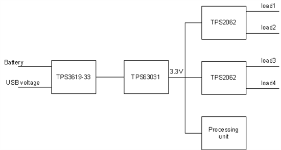
  • I'm afraid I cannot post here the full layout nor the schematic of the board. Attached, though, you can find the block diagram of the power management block.


    During sleep, normally only the processing unit receives voltage. You can ask me more details if you need. One thing that I noticed about the schematic, is that I haven't used two 10uF output capacitors but only one. Is this a problem?

    I hope that soon I will post the waveforms that you asked me, too.

    Regarding the current consumption. I am measuring the total current consumption that is drawn from the battery, with the help of a voltmeter. But I assume that this is also the current consumption of the regulator. The processor's current need during sleep is below 1uA.

    About testing it at other input voltage values : Above 3.6V (4.2V or above), the current consumption during sleep is kept under 1mA and around 600-700uA. However, when I tried to operate it with voltages below 3.6V I have seen the following : The current that I measured is above 5.5mA. It rises at about 6.7mA @ 3.0V input voltage. And the current during the active periods is higher than 50mA, too. Moreover, while the board is in sleep and the current is about 5.5mA, I started lowering the input voltage from 3.6V towards 3.0V and the current changed too, simultaneously. If, while in sleep, I started rising the input voltage above 3.6V towards 4V, then the current became lower, (around 3mA) but after one active period, the current went to around 600uA.

    And lastly, something very curious. When I operated the board with 3.0V and the board tried to go from sleep to active, it seemed like the regulator couldn't give the necessary current (operating in boost mode). The board never went to active mode and a strange periodic whistle could be heard (I assume from the inductor???). And in fact, the on-board memory seemed to have been destroyed by this.

    Is there any chance that this weird behavior is caused by heat? And probably it seems as if the regulator cannot provide more current than around 60mA. I will try to post the waveforms soon, too.

  • I wanted to touch base with you and see if you were able to take the requested scope shots.

    Unfortunately I really need to be able to see your schematic/layout to do some proper diagnosis. Since posting them is not an option could you provide insight into this particular areas?

    1. Output Capacitor Value and Placement: What size, value, and material cap are you using? What voltage is it rated for? Where is it placed on the layout?

    2. Inductor Value: What inductor are you using?


    To answer your questions:

    The single capacitor shouldn't cause any major problems if it is sized correctly, but there are a wide variety of factors that can change the value of a capacitor. Providing an answer to the question above should be able to rule out if the output capacitor is a problem or not.

    The symptoms you are listing do not sound like it would be heat related. An overheating issue would cause the device to shut down when the temperature exceeds the absolute maximum.