This thread has been locked.

If you have a related question, please click the "Ask a related question" button in the top right corner. The newly created question will be automatically linked to this question.

How does over current circuit work in the TPS40210?

Other Parts Discussed in Thread: TPS40210, TPS2010, SWITCHERPRO

Hello:

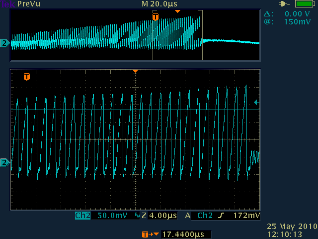
I'm hoping someone can explain the specific conditions that cause the over-current circuit in the TPS40210 to shut down the supply.  The datasheet say if the ISNS pin sees a voltage over 150mV the supply will shut down.  However, it doesn't say if one pulse will cause it to shut down or if the condition has to persist for a certain amount of time (or pulses).

My current design is feading a load that takes periodic transient currents. During these transients I see the voltage on the ISNS pin start to rise, but the supply doesn't shut down until the pulses are around 230mV. 

My question is this,  why are the pulses reaching 230mV? Is the chip out of tolerance, or is it because the current is getting that high during a time out period.  If there is a time out period, what is it based on, and can I change it?

  • I edited the title of this post to reflect the correct part number of interest--the TPS40210, not the TPS2010.

    As shown by the block diagram on page 11 of the datasheet, the ISNS signal goes straight into an OC comparator with a reference voltage of 150 mV typical.  It only takes a single pulse to trip the OC limit.  There is also some amount of leading edge blanking implemented on this signal.  This time begins at the beginning of each switching cycle (when the gate drive goes high) and prevents the IC from declaring an OC condition for the duration of the blanking time.

    Both the nominal voltage trip point for the OC circuitry and the blanking time have a tolerance associated with them.  The trip voltage tolerance is specified and guaranteed, but not the blanking time.

    The 150 mV must be measured directly at the pins of the IC--from pin 7 to pin 6, with a low inductance probe.  Using a clip lead and ground clip wire adds additional noise to the measurement and is not accurate.

    An RC filter between the sense resistor and IC is strongly recommended and can delay an OC event.

  • "It only takes a single pulse to trip the OC limit"

    I'm seeing roughly 50 pulses after the ISINS pin reaches 150mV.  The last pulse before turn off is 230mV.  The last 30 pulses or so are above 180mV.  


    I have a differential probe right on the pins, and I'm seeing pretty clean pulses with very little noise.  It really seems like there's a time out period, or the over current is tripping at around 230mV.


  • Could you attach a waveform of 2-3 pulses?

    Have you tried using a non-differential probe?

  • Patrick,

    I am verifying with the IC designer whether the controller has a fault de-glitch counter or not.  I do not believe it does, but want to confirm for certain.  If the device does have a de-glitch counter it is either 3 or 7 cycles.

    Most likely what you are observing is an unintentional affect of blanking and propagation delay resulting in the peak voltage exceeding the threshold voltage.

    When an OCP even is detected, there is a delay for this comparator single to propagate through the fault detection circuitry back to the PWM and turn-off the low-side driver.  If the PWM is terminated normally by the PWM comparator during this propagation delay, the OCP fault is not declared.  As a result, the ISNS voltage must be greater than 150mV for a period of time for OCP to be declared (I am checking on this approximate delay)

    As a result, there is a slight dependance of the actual over current limit peak ISNS voltage on the slope of the ISNS.  As the over-current condition increases above the DC threshold, providing more over-drive and reducing the propagation delay.  The 230mV that you are seeing in your application is likely the intersection of the rising peak voltage and the decreasing propagation delay that results from increased sense signal.

    Based on that, there is a way to improve the accuracy and effectiveness of the Over Current Protection circuit - decrease switching frequency and increase inductor value.  This will both increase the available sense time and decrease the rise in current during the propagation delay from OCP trip sense to OCP fault declaration. 

  • Here's the waveform at the ISNS pin.  I zoomed in on the last few pulses.  I doubt any ill effect is due to noise. 


    The horizontal cursor  in the zoomed in picture is at 150mV. As you can see there's quite a bit of pulses that occur after 150mV has been exceeded.

    The reason I'm looking into this, is because I actually would like to extend the response time so that I can allow for some transient currents on the load, and not have to increase my trip point.

  • Patrick,


    Thank you very much for the waveforms.  This looks to me like almost exactly what I described.  The early pulses are not exceeding 150mV for a long enough time to respond to the peak voltage, resulting in a failure to trigger the OCP fault prior to the PWM termination.  There are a few things you might be able to do to help this:


    1)decrease the bandwidth of the ISNS filter R-C.  This will slow the rise of the of the sense point slightly, which will reduce the peak sensed voltage and allow a little more OCP level.  Its possible to add sufficient filter to ISNS pin to trigger only on average switch current, however this also results in average current mode control in the PWM and is generally undesirable.

    2) further decrease the inductor value to increase the rate of rise of the inductor current.  This will cause the ramp to be faster achieving a higher peak current before OCP has occured long enough to trigger OCP, though I don't recommend counting on such a propagation delay as it is not characterized and could from device to device and over temperature.

    3) Another solution would be to add a divider from the current sense resistor to ISNS to GND.  Add a capacitor divider from the sense resistor to ISNS to GND.  At high frequences, such as the switching frequency, the capacitor divider would dominate and provide the necessary AC ripple for PWM control.  At low frequencies the resistor divider would dominate, to provide a DC current trip point.  The transition between the two would occur at a pole and zero formed by the two R-C filters.  By making the AC gain lower than the DC gain, you would effectively add a time-constant to the current limit function.  You'd need to use the high-frequency (capacitor) gain for the control loop and keep in mind that you're adding a pole and zero to the loop response, so you don't want to mis-match the dividers too much.  A 2:1 resistive divider and 3:1 capacitive divider for example, should be close enough to minimize the phase impact between the pole and zero while providing a higher transient current limit but maintaining a lower DC current limit.

  • Pete:


    Thank you for your detailed responses. You've been a huge help!   Given that my transient conditions last a long time (over 100 cycles) I think I'll need to try average current control.


    Thanks again.


    Patrick

  • If you used the following combination:

    100kOhms + 100kOhm for the resistor divider (you would need to double your sense resistor)

    22nF + 10nF

    You'd have a pole at about 300Hz with a zero at about 450Hz as the attenuation of the divider shifts from 1/2 to 1/3.  There would be a slight dip between the two frequencies, but only about 10 degrees or so, so as long as the loop is fast enough to keep that well above the cross-over frequency that shouldn't be an issue.

    for loop response, you'd want to calculate as if the resitor was 10/32 of it's actual value (after doubling) since the capacitive divider is going to dominate the loop response.  This would provide an additional 50% current limit with a 1ms time constant.  Would that be sufficient to ride through your over-current condition? 

  • I confirmed with the design group - The TPS40210 does not have an OCP fault counter.  A single detected OCP fault will result in shut-down.  The increased peak voltage that you are observing is a result of the propagation delay of the OCP fault signal from the ISNS pin to the internal OCP fault logic

  • Pete:

    Thanks for all your input.  As I investigated my design, I realized that my inductor was substantially undersized.  (I used SwitcherPro to design the supply, and it picked a 1µH inductor when it should have used something around 10µH.)  Because of this I had an enormous ripple current and that was amplifying the surge in the load and making it look worse than it really was. 

    Now that I have the correct inductor, the supply has enough overhead to allow for the transient currents in the load without resorting to any of the options we've discussed above.  

    Thanks again for looking into this for me.

    Patrick


  • This is a known issue with the SwitcherPro component selection criteria for the TPS40210 that will be corrected in the next release of SwitcherPro.


    I am glad we've been able to address your issue.  Please contact us through the TI Forum if there is anything additional we can assit you with.