This thread has been locked.

If you have a related question, please click the "Ask a related question" button in the top right corner. The newly created question will be automatically linked to this question.

Cascading TLC5917

Other Parts Discussed in Thread: TLC5917

Hi,

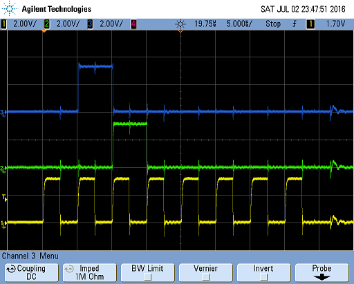
We are designing a digital display sign and are prototyping using TLC5917s, we have used these before on other projects without a problem though they have all be in one cascaded screed. In this job we have 8 TLC5917s cascaded on each board and are trying top cascade multiple boards but the clock and data seem to be out of sink. We looked at this on our scope and we have the the rising edge of the clock bang in the middle of the data bits on the input to the first chip, however on the SDO data out from the first chip the relationship between the clock and data has shifted by almost half a clock cycle (on the first chip) and now the data bit is just getting sampled by the clock. This is replicated over the next seven TLC5917, they all work but it just looks wrong having the rising edge of the clock right on the edge of the data pulse. When we try and drive the second board through a buffer IC the tiny delay caused by the buffer is enough for the next board to miss the correct slot and clock the data into the next bit in the register. We have slowed down the SPI to 200K but this makes no difference. We were planning on using several hundred of these per sign, but seem to have hit a brick wall for the moment. Any advise appreciated.

  • Hi Philip,

    I'll be glad to help with this problem, but please keep in mind that the 4th is a holiday, so this might take a few extra days since I'm away from the lab.

    In the meantime, can you please share the oscilloscope images you took. A schematic would also be helpful to make sure I'm understanding the setup conditions.  

  • Hi Harry,

    I have attached schematic showing the cascade wiring and IO between PCBs. Also attached are two scope captures. I have set up sytem to write one byte 0x08, every second to allow simple screen capture.


    Yellow trace clock into 1st TLC5917, Green trace data bit that has been sent SDI, blue trace is SDO from 1st IC feeding SDO of second IC. The ICS on the same PCB share the same clock and they seem to be okay with the blue pulse though it does seem to be right on the edge of the rising edge of the clock. We have eight of these ICs cascaded on each pcb.

    We have a buffer icsn74lv07a on the clock and data lines between PCBs. We are looking at changing this for push pull topology.

    Second trace shows the same signals on the 1st TLC on the second PCB

    Schematic showing cascade.

    Thanks in anticipation.

    Phil

  • Just noticed a small typo.

    The SDO from the first IC does feed into the SDI on the second TLC chip.

    Phil