This thread has been locked.

If you have a related question, please click the "Ask a related question" button in the top right corner. The newly created question will be automatically linked to this question.

TPS92410/ TSP92411 based desigh dimming problem

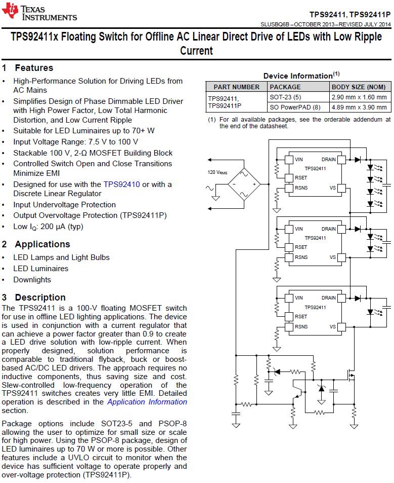
Other Parts Discussed in Thread: PMP6021, TPS92410, TPS92411

Hello!
I tried to do LED driver board based on PMP6021 document. It works, but I have the problem - when I try to use ADIM input (with potentiometer or from external voltage source), I see the LEDs are dimming, but not linear for values of input voltage lower than approx 0,3V. Also some segments have different brightness.
The values of elements are equal to PMP6021.
What may be wrong?

PS Triac dimming also works incorrect for small dimmer values

  • Hello,

    It should be linear until the shutdown point. Are you analog dimming this with the input from a Triac dimmer?

    Also, there is a pull-up resistor on Adim, if your potentiometer is a fairly high value R17 may need to be removed. PMP6021 is a non-isolated design and there can be interference with test equipment that is ground referenced as well.

    Thanks,
  • Hello,

    As for the triac dimming, at deep dimming levels the upper stack will be the first to drop out due to the input voltage not being high enough. Or are you seeing something else?
  • Hello!
    Thanks for your answer.
    I found some issues in my prototype.
    I changed my design to 3-stack schema. Rsns is 1M and Rset of stacks was calculated by slvc580 Excel calculator. (1.91M, 1.82M, 1.69M)
    I got minimal dimming power 1.5W for full power 18.8W (dimming range 8%-100%).
    I used ADIM input, and when I set input voltage below 50mV the LEDs was shutdown as it should be. I tried to use TSNS input for dimming, but minimun power was 1.1W at 0 input and LEDs never off.
    How can I increase dimming range ( for example, to 5%-100% ) and use ADIM shut down functionality?
  • Hello,

    You can add a high value resistor from Vref to CS pin (pin 10 to pin 5).  This will offset the current command slightly.  You can try a 3.0 Mohm to start and see if that makes a difference and adjust from there.  It should offset about 50 mV if the inline CS resistor is 54.9 Kohm.  It is R29 on PMP6021.

    You may also see the LEDs somewhat on due to the Rsns resistors.  If this is the case you may need light loading across the LED stacks to turn them fully off.

    You can also use Tsns to dim and Adim to turn the LEDs off.  Tsns and Adim function the same except for the turn off threshold of Adim, Tsns does not have that.

    Thanks,

  • Thank you for help!

    I tried the first variant - now I increased the full power of light module to 29,8W and when I set 3M resistor the dimming threshold decreased to 1,3W. So, dimming range now 4%-100%. Excellent!

    But now I have a strange effect - when the control voltage decreases below shutdown threshold, the top stack LEDs still have a small glowing. If I turn off device (by mains switch), and then turn it again I see what top stack LEDs smoothly increases its light in some seconds after powering. In this mode device doesn't have measurable power consumption (by electronic wattmeter). All other stacks are off.
    I think, it is not due with dimming, right?

    I did not fully understand the secont variant. Can you explain it more detail?

    The third variant unfortunatelly is not applicable, because I have only one PWM output, which I use for light control.
  • Hello,

    It is related to dimming because of the currents needed for Rsns and/or the upper transistor feeding the TPS92411 Vin. These currents are small and don't affect anything at full power but at very low dim levels you can see it. The TPS92410 is off, the current is running through the Rsns resistors.

    My second comment is about what you are seeing though I think it may just be because of how Vin to the top TPS92411 is generated. Is only half of the upper stack glowing or the whole stack? If it is half of the stack it is because of the transistor that generates Vin for the top TPS92411. A high value load resistor will divert this small current away from the LEDs. If it is just half of the upper stack something like a 4.99 Mohm across the half of the upper stack may be enough.

    If it is the entire upper stack it is caused by the Rsns resistor on the lower two TPS92411s. These draw a small amount of current that has to run through the upper stack. If this is the case then the entire upper stack needs a high value resistor across it to divert the current away from the LEDs. You could try a 1 Mohm across the upper stack to start with, I would use a 1206 as the smallest size due to the voltage rating. See if the issue goes away or if it reduced a lot.

    Thanks,
  • Thanks for your help!
    I connect 1M axial resistor to opposite point of top stack and glowing effect was gone.

    I trying to increase power of module up to 250W. Can I use one TPS92410 with appropriate MOSFET and 2 sets of TPS92411?
  • Hello,

    You cannot use the TPS92411 set of strings in parallel with one MOSFET.  The MOSFET is absorbing the voltage difference between the input voltage and the total TPS92411s open.  Two sets of strings will not switch at the same point meaning to different current regulators are needed.  This can be Two TPS92410s and MOSFETs or you can add an additional MOSFET connecting the gate to the TPS92410 gate drive and using the same current sense resistor (though it is not connected to CS, it would be open loop).  This relies on the Vgs threshold to be similar.  To add additional margin more resistance can be added to the MOSFET source of the MOSFET that is connected to the CS input of the TPS92410.  It would look like a resistor divider from the source to ground with the center going to the CS pin through the 50K to 55K ohm resistor.  The second MOSFET would have a single resistor from source to ground that was the sum of the two resistors from the regulating MOSFET.  If Vgs threshold is close the current through both MOSFETs will be almost the same but they will have independent drain voltages.

    125 watts per string set is very high for the TPS92411s.  It might work with four string sets at 62.5 watts each depends on how well it dissipates heat.  Is this with the SOT23-5 package or the larger eight pin SOIC?  The MOSFET has a two ohm on resistance.  At 125 watts the peak current through the string is around 750 mA assuming 240 VAC input.  If the TPS92411 MOSFET is hot the voltage drop across the MOSFET when on can be above two volts.  You may find you can run higher currents through the TPS92411s it just was not intended to go that high in power.

  • Thanks!

    We using the TPS92411 in SOT23-5 package.
    Why current for 240V and 125W is so high? How we can empirically calculate current through TPS92411 by power? What rated current is for TPS92411 in SOT23-5 package?
  • Hello,

    Peak current for 240 volts at 125 watts is (125W/240V*1.414) = 736 mA. This is power factor corrected so near the peak of the AC voltage the current is near the peak (sinusoidal). From an RMS standpoint the current is much lower in the TPS92411. The limitation for current is around 500 mA for proper operation provided the part can dissipate the heat generated. I would keep it in the 200-300 range just because I like having quite a bit of design margin.

    As for calculating current I have a Mathcad spreadsheet that could be modified to do this. It is probably easier to watch the current waveform and watch when the TPS92411 is closed and calculate it from that.

    Thanks,
  • Hello!
    Thanks for answers!
    But I used calculator from TI "slvc580", which has the note "This design is good for 1.6W to 100W of input power" and for 100W light power is approx 88W, so the peak power is approx 88W/240*1.44 = 0.52A
    This is correct? Or in this case we must to use SOIC package? Which current limits for SOIC?
    We need to implement 100W of light power module minimum...
  • Hello,

    The front page of the datasheet states 70W or possibly more in the features and further down in the description (this is for both TPS92411 packages).  We didn't intend to go beyond 35 watts at 120 VAC and 70 watts at 230/240 VAC.  The peak current at 100 watts input will be 100W/240 VAC * 1.414 = 0.59A.  The efficiency is mainly lost in the current regulating MOSFET, that current still runs through the TPS92411s so it needs to be calculated with input power not output power.

    There really isn't a current limit for the TPS92411 however it will begin to hard switch if the current gets too high meaning EMI will go up significantly.  If I recall this limits the  useable current range to 500-600 mA.  You can try to do this but will most likely have to use the SOIC and heatsink it fairly well.  There is more than conduction loss with this part due to slew rate control.  Even though there are only a few switch cycles per half line cycle the transition is slow which results in switching loss.  You can watch the slew with an oscilloscope and calculate the power loss from that or use the datasheet values for slew rate.

    An example would be TPS92411 open loss per switch cycle on the 80 volt stack.  Slew rate is 0.5V/uS so 160 uS to transition.  At 120 Hz this duty cycle is almost 2% for this one transition.  The TPS92411 close switch loss will be half due to the slew rate being 1V/uS.  Average power dissipated during the open switch slew would be 80V * 0.5A / 2 (/2 is because the voltage is slewing from 0 to 80) = 20W.  At 2% duty cycle this is 400 mW for that one transition.  Add half again for the close loss and it's 600 mW.  There are two on/off cycles on the 80 volt stack though the current during the other two transitions will be lower.  Add to this the RDS on loss the part will have to dissipate over one watt.

    The cascode MOSFET for the 160 volts stack will have to increase in size as well.

  • Hello!
    Thank you for explanation!
    I'll read datasheets more precisely.
    When I tried to calculate power loss of switching for our design on 500mA I got a 1,44W for middle 80V stack and 0.84W for bottom stack.
    As I understood, we can to use cascode circuit like in top stack with appropriate MOSFET for increasing of current and limit its slew rates, but it increase the size and reduce efficiency (increasing power losses for switching), right?
  • Hello,

    No, a larger MOSFET will not increase switching losses because the slew control is external and there are very few switching instances.  Switching loss is controlled by C3 on PMP6021.

    The cascode MOSFET may get bigger but the losses will go down because of RDSon.  The switching loss is a function of the slew control, which is external on the cascode MOSFET and something to consider when choosing the MOSFET.  Unlike a power supply where Coss increases switching loss it is negligible here due to how few switching cycles there are.  The slew control is done with C3, R6, D16 and Q1 Vgs threshold on PMP6021 design.  The turn on and turn off slew rate is depending on Vgs threshold, on this it is around four volts.  It may not be obvious how this works, I'll try and explain.

    The gate of the cascode MOSFET is held at 12 volts via D16.  When the TPS92411 MOSFET closes the gate the voltage across R6 becomes 12 volts minus Vgs threshold, or Vgs threshold minus 12 volts depending on the polarity direction you chose, eight volts or minus eight volts.  The current from C3 (I=C*dv/dt) cancels the current through R6 to hold the gate constant (this is the MOSFET closing slew control).  In the other direction it's just the Vgs threshold so switch opening R6 voltage become Vgsthreshold, about four volts meaning I=C*dv/dt is opposite polarity and about half the slew rate.  This is to try and keep it matching what the TPS92411 does.

    If the Vgs threshold was six volts the slew would be about the same for turn-on and turn-off which is not desirable.  If Vgs threshold was 1 volt the ratio gets too large and to dial in the correct slew for turn-on the turn-off would be much too long hurting efficiency.  The zener voltage and Vgs threshold control the ratio of the slew.  R6 and C3 control the rates of these slews.  Reducing C3 or reducing R6 will make the upper stack slew faster.  Efficiency will go up but so will EMI, it's a balance between the two.  In your design you may be able to reduce C3 and increase the Rectified AC EMI capacitor since this in not a triac dimming solution.  It can only be reduced so far before it affects the other TPS92411's operation.

    Thanks,

  • Hello!
    Thanks for your answer.

    I set the voltage thresholds for all 3 stacks like in TPS92410EMV-002.

    Unfortunately, I incorrectly asked. Sorry for my poor english

    I mean, can we use cascode circuit like in top stack, for middle and bottom stacks for increasing of LED current and power? How to calculate the parameters of circuit elements for this? And how this affect to flicker characteristics?
  • Hello,

    Yes you can do that.  Since the slew control is V/uS on all channels the circuit can just be replicated on the other two channels.  Rset and Rsns remain the same for all channels (if you have not changed the stack voltage).  The switching loss will determine how much power the cascode MOSFET must dissipate.  Upper stack has one turn on and one turn off transition, the middle has two of each and the bottom has four of each.  It should not affect the flicker characteristics.  You must also make sure the cascode MOSFET can handle the SOA of the switching transition.

    Thanks,

  • Hello!
    Thanks for your help!
    Can you help me with power loss calculation for current regulator MOSFET?
    I trying to make schematic for 100W of light power, approx 113W (calculated by slvc580) of input power on 240Vac. As I understood, the peak current through TPS92411 cascode will be 113W/240V*1.414 = 0,67A. And all voltage drop will be on current regulator mosfet, for example when all 3 stacks are open: 240V*1.414 - 168-84-42 = 46V. For current 0.67A peak power will be 46V*0.67A = 30W but I don't know duration of this event.
    How I should to select appropriate MOSFET?
  • Hello!

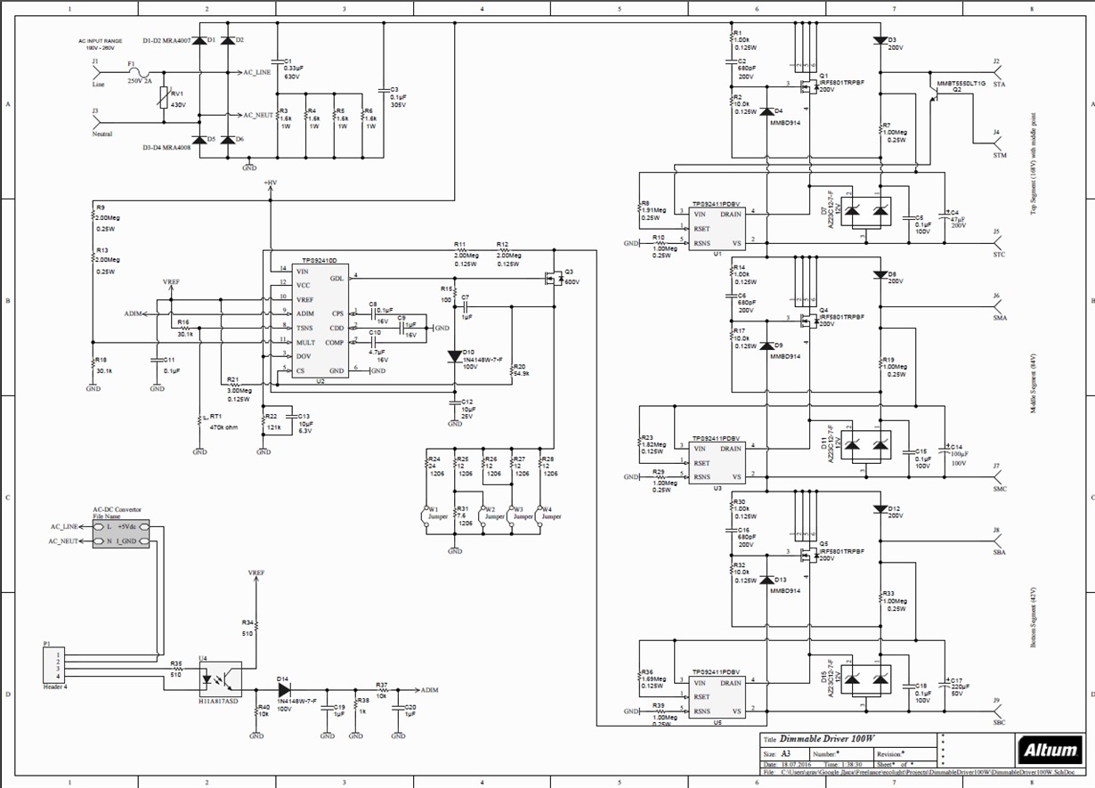
    I tried to make schematic for the 100W LED driver with cascode amplifiers.

    Can you see this schematic and say what I need to improve?

  • May we increase the power of driver to 500W?
  • Hello,

    It's actually quite a few equations to calculate that but it's done in the excel for the efficiency calculation. I assume if the output is 100 watts and the input is 113 watts (it will be more since this is only ideal input line condition) the MOSFET power will be 113W - 100W or 13 watts. At high line it will be more. 264 VAC * 1.414 - total stack is 79 volts, times 0.67 amps = 53 watts and it is in the 111 state longer so you can assume about double the power in the MOSFET. At this high of a power level I would try to go to four stages.

    Things to watch for:
    MOSFET SOA, very important. During start-up the capacitors across the LEDs are discharges so all of the input voltage is across the MOSFET. It needs to be able to handle 0.67 amps with the rectified peak voltage during the capacitor charge time.
    MOSFET heatsinking, unlike a power supply that dissipates power in many components this dissipated a majority of the power in one component. 20-30 watts requires quite good thermal interface and heatsinking.

    Thanks,
  • Hello,

    You can remove the damper circuit if you are not triac dimming. That's the four resistors and capacitor by the rectifier bridge. The EMI capacitor will need to grow. I would start with 1.0 uF for 100 watts (this will get determine during EMI testing). The cascode MOSFETs need to be larger. The part on the schematic is meant for up to 20 watts. The electrolytic capacitors will need to get much larger if you want to keep the ripple fairly low, to keep the ripple similar the values would scale up by the power level (five times the power would be five times the values). From previous experience you may want to add a small (say 0.1 uF) capacitor from the upper TPS92411 Vin to Vs (pin 3 to Pin 2).

    Not sure what you are doing with the opto-coupler, hopefully not running it in linear mode since it looks like it is set up that way. Also, not sure if your dimming signal is a 'UL safe' voltage. If it is it may not want to be on the came connector as the AC (creepage and clearance).

    Thanks,
  • Hello,

    I suppose it can be done but not sure if I would. I would not only add a fourth stage but a fifth as well if I were to try this. The other possible issues is finding a current regulating MOSFET that can meet the SOA and can have enough thermal dissipation.
  • Hello!
    Thanks for help!

    I selected some candidates for MOSFET of cascode circuits - IRFR220N (Infineon) and FDD7N20 (Fairchild) in DPAK package. Can you tell me it is fit to 100W driver?
  • Hello,

    You can try them both.  The IRFR220 is an old part from International Recifier.  The RDSon will increase with temperature as well.


    Thanks,

  • Thank you!
    You're right, but IRF became Infineon now...
    How about current regulator MOSFET? DPAK package is enough for continuous dissipation of power or we need to use 2 MOSFET in parallel?
  • Hello,

    For the current regulator, at 100 watts, the part has to be able to dissipate a lot of power AND must be within the SOA (safe operating area) of the MOSFET.  At 100 watts it will be a fairly large die part and you may want to go to a larger package to dissipate the heat.  If worst case the efficiency is 80% about 25 watts will have to be dissipated in the current regulating MOSFET.

    Since the MOSFET is in linear mode you cannot just parallel them.  It takes a bit more to do that since the Vgs threshold can be slightly different and Vgs threshold drops with temperature meaning one MOSFET would take all the current.

    Either one large MOSFET or a main MOSFET with slave MOSFETs and possibly added resistance in the source to force current balance between the parts.

    Thanks,

  • Hello!
    Thanks for explanation.
    As I understood, any package like DPAK and D2PAK is able to dissipate up to 85W depending of ambient condition.
    But next limit is the SOA. Our MOSFET must be able to operate with approx 0.8A at approx 350V on DC current, right?
    So if it right, minimal appropriate MOSFET which I found, is STB24N65M2 (datasheet has some bugs in SOA figure) and STB24N60M2.

    So we have the cost increasing 10 times...

    About circuit with optocoupler - it is my attempt to make a PWM to analog conversion for dimming control
  • Hello,

    Yes, the STB24N65 curve is off (probably will work since it's probably the same die as the STB24N60), the STB24N60 would work. Note that those curves assume the junction is starting out at 25 Celsius so a bit more margin might be good. Remember also that 350V at eight amps is during the peak of the rectified AC so there is some margin in this since the average current will be around 0.5A. The time is determined by the value of the capacitors.

    I'm not sure how you are dealing with the thermal management of this but dissipating 25 watts in a D2pak should be looked at, that's a lot of power for a D2pak.

    Thanks,