This thread has been locked.

If you have a related question, please click the "Ask a related question" button in the top right corner. The newly created question will be automatically linked to this question.

LM5175 possible noise Problem

Other Parts Discussed in Thread: LM5175, LM5175RHFEVM-HD

Hi, 

I'm having troubles using TI's LM5175. After cheking there's no error on the schematic, and since the nauture of the problem seems difficult to understand, I examine each part of the circuit separetly. First, I try to unferstand the BUCK converter branch.

This is the schematic (it has some probes defined in order to understand the further osciloscope captures).

The circuit is designed to drive up to 5A @ 12V.
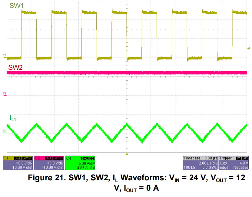
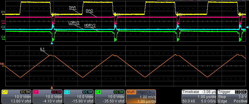
On BUCK phase, I get spected results as long as Iout is lower than 4A aprox. These are the corresponding waveforms:


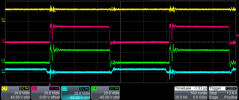
It's worth noting the 2 step linear voltage drop on Gate and Source of the MOSFET (red and green probes) right after MOSFET's activation. I guess this is a clue of some of the missbehaviour.


When Iout is approximately 5A, this is the corresponding waveforms:

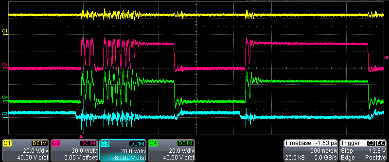
This is a behaviour difficult to understand. It seems the Gate of the MOSFET is not able to mantain it's status during activation.

I would thank you all for some guidance or any kind of helpful information.

Best regards.

  • Hi Israel,

    I think there is another post with similar question.
    This requirement is quite similar to LM5175RHFEVM-HD. I suggest using that as your initial evaluation platform. Please also look at this guide on switch node ringing.
    Controlling switch-node ringing in DC/DC converters - EDN
    www.edn.com/.../ViewPdf

    Hope thsi helps.
    Regards,
  • Vijay, 

    Thank you very much for your answer.
    I'm still reading your guide about switching-node ringing in DC/DC converters.

    Meanwhile I read the LM5175RHFEVM-HD evaluation guide to use it as a reference as you told me.

    This caputre is extrated from the evaluation guide:

    I've tried my PCB under the same conditions to establish a comparison and this are my results:


    (IL1 has just a qualitative value since its mesured using algorithmic functions of my osciloscope. I think it's enough to understand it's behavior).

    Firstly I just mesured SW1, SW2, and IL1, as on the picture of the guide. But after notticing the strange behavior of SW2, I've also mesured LDRV2 and HDRV1, to understand better if there's an activation of the side2 MOSFETs. As far as I know, during BUCK regulation side 2 MOSFETs should not be working, thus meaning that QL2 should be OFF and QH2 should be ON.

    I would agree any kind of indication abou the nature of this behavior.

    Thank you very much for your time.

  • Hi Israel,

    I think the FET you are using have lot of QRR and (potential for) ringing on SW nodes. You may have to resort to the schemes shown in Figure 10 of the guide in the link I shared before.
    In particular a zener clamp (8.2V) across CBOOT2 should help protect the gate drivers.
    You should also replace the controller IC. I suspect the ringing induced overvoltage on CBOOT2 is causing this.

    Thanks and regards,
    Vijay
  • Hi Israel, I have your exact same problem and I can't find a solution... Have you solved your issue?
  • Gianluca,

    Hi. After reading Vijay's indications, I read carefully the related documents, concerning snubbing and ringing on SW nodes. I'm sure the gate voltage my circuit presented to the IC was not in the correct range due to this problems, so I somehow broke the drivers.

    My conclusion is that you have to be extremately careful while designing with this IC, and take all the extra protecions indicated by Vijay's application document.

    I didn't solve the problem. IHopefully, I had the chance to redesign the PCB with another solution.

    Sorry.