This thread has been locked.

If you have a related question, please click the "Ask a related question" button in the top right corner. The newly created question will be automatically linked to this question.

Question about LM5574 maximum rating (SW to GND)

Guru 19595 points
Other Parts Discussed in Thread: LM5574, LM46000

Please let me know about two points below of LM5574 maximum rating.

①Is there spec information of SW to GND transients?

 For example, LM46000 datasheet page-4 described "SW to PGND less than 10ns Transients".  (see below)

 Customer want to know SW to GND transient spec of LM5574, too.

 ※Background is below, undershoot is -3.1V.

②LM5574 datasheet page-3 is described "SW to GND (Steady State)".

 What mean of steady state?

 Is this condition include undershoot?

Best regards,

Satoshi

  • Any update on this?
  • The LM5574 datasheet only includes the steady state limit of -1.5 V.  Steady state means dc value (about -1.1 to -0.9 V in your waveform).  Probably all SMPS will show similar transients as you show and many datasheets will include a transient specification as well as the steady state rating.  In any case I wll move this to the Simple Switcher forum where you may get additional response.

  • John Tucker-san

    Thank you for reply and move forum.
    I looking forward to update in this forum.

    Best regards,
    Satoshi
  • The 'steady-state' spec on the datasheet means DC value. It does not include understood during switching transitions. The undershoot seen on the board depends on the rise/fall time, Vin, load and PCB layout. How the switch node is probed also affects the amount of the undershoot seen by the scope. We can review the layout if preferred by the customer.

    Best,

    Yang
  • Yang-san

    Thank you for reply.

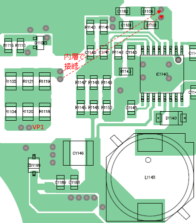
    Schematic and Layout is attached below, 

    ※Red line: connecting from inner layer

    I think that Cin is long distance from LM5574.

    If there find the other careful point, please let me know.

    By the way, probe is no problem because customer is careful with probe's GND loop.

    Best regards,

    Satoshi

  • Hi Satoshi-san,

    I agree the Cin capacitors should be closer to the IC, especially the GND node of the caps. The current going through input capacitors in buck converter is discontinuous current. Minimizing the loop area from Vin pin to CIN caps back to IC ground is critical in reducing switching noises. I'd suggest flip the CIN caps horizontally to make the GND nodes closer to IC ground. Vias add additional parasitic inductance and it will increase ringing level during current transitions. CIN ground nodes tie to IC ground on top layer with short thick copper trace is recommended.

    The red internal connection for VIN also carries noisy discontinuous current. It is recommended to move the resistor bank of R1105/1104/R1121/R1120/R1119/R1118 closer to CIN. And run the VIN trace with short thick copper trace on top layer as well.

    Another recommendation is to reduce the copper area of the FB node. FB node is a sensitive signal node. Ideally, the FB resistors should be place as close as possible to the FB pin and trace to the FB pin should be short and thin. The copper area for FB node should be minimized to reduce capacitive coupling of noise.

    C1189 and C1188 are high frequency bypass capacitors at the output side. Output side is not as noisy as the input side in buck converter. It is still recommended to place C1189 and C1188 ground node closer to the IC ground.

    Traces into IS pin should be thicker if possible, since it conducts pulsing current as well.

    Hope this helps.

    Regards,

    Yang