This thread has been locked.

If you have a related question, please click the "Ask a related question" button in the top right corner. The newly created question will be automatically linked to this question.

UCC27201A-Q1: Reg Issues with UCC27201A-Q1 part

Part Number: UCC27201A-Q1
Other Parts Discussed in Thread: UCC27201A

Dear All,

one of my customer using UCC27201A-Q1 part for battery tester product, they are facing some problem due to UCC27201A-Q1 with thermal pads. 

1. At long run the IC gets hot and fails. Wondering if thermal pads are any issue.

 2. If the output of this synchronous buck converter is terminated by very small resistance (say fully turned on  MOSFET with resistance of 40mOhm) the gate of high side MOSFET draws huge currents like 1.8A. Couldnt figure out this behaviour.

Request you to advise your feedback.

Rgds,

Aravind.

  • Aravind,

    I have asked one of my colleagus in the drivers team to look into your question. You should get a response within the next day or 2.

    Thanks,
    Bernard.
  • Aravind,

    I am an applications engineer with the gate driver group. The behavior you describe is not typical. In order to better diagnose the issues you are experiencing, I would like to ask for some information regarding your implementation:

    a. How is the UCC27201A-Q1 being used? From your bullet-point #2, it seems perhaps it is driving a synchronous buck converter. Please confirm.
    b. What are the parameters -- VDD, frequency, load MOSFET, etc. Providing a schematic would be most useful.
    c. Is the design implemented on a printed circuit board, or is this hand-wired/bread-boarded?

    Regarding your two items:

    1. The answers to the questions above should help me understand possible source of heating. Does anything change in the running conditions between startup time and when the device fails? I notice you mentioned at long run -- how long a running time is that? Does the device get hotter and hotter over time, or does it get hot suddenly just before failure? The thermal pad is meant for heat-sinking of the gate driver. Proper connection to a copper ground plane on the PCB will greatly improve thermal performance.

    2. If the output of the buck converter is connected to ground via a small resistor such as 40mohm, it makes sense that a very high current is drawn through the high-side MOSFET. Whenever the high-side FET is on, a very low impedance path to GND is created though the rDSON of the FET (which is typically very small), and the 40mohm resistor. Please let me know more details about what you expected from this circuit so I can help debug.

    Regards,

    Daniel
  • Dear Sir,

    Thanks for your reply. please find reply as below

    1. UCC is driving synchronous buck.

    2. Vdd is 12V, freq 33kHz, MOSFET used is IRF150n or STW40NF20 (not as in attached schematics).

    3. Circuit is on PCB.


    We have tried varying the gate resistances of HI and Lo sides from 4.7ohm to 1K.

    Gate to source resistor is 10K.

    Snubber is not populated. 

    Rest all as per schematics.

    Attaching the schematics for further reference.


    Rgds,

    Aravind.

  • Aravind,


    Thank you for the additional information. The schematic looks correct to me. I do recommend that you change C103 to an higher voltage-rating component for reliability purposes, but that should not be an issue with the overheating you report. I will ask one of my colleagues to take a look as well to get another set of eyes on it.

    Is the FET at the output meant to conduct via its body diode, to a load? I do not see an issue with that, per se. However, you mentioned a high current when this FET is installed. Please confirm: the same behavior is not observed if instead of the FET, there is a direct connection (short) to the load.

    Does anything change in the running conditions between startup time and when the device fails? I notice you mentioned a long run -- how long a running time is that? Does the device get hotter and hotter over time, or does it get hot suddenly just before failure?

    Other places I would look are the VDD and HB supplies. When you check with a scope, are they remaining steady, or do they fluctuate? The HB supply needs to be rereshed periodically by switcing on the low-side FET.

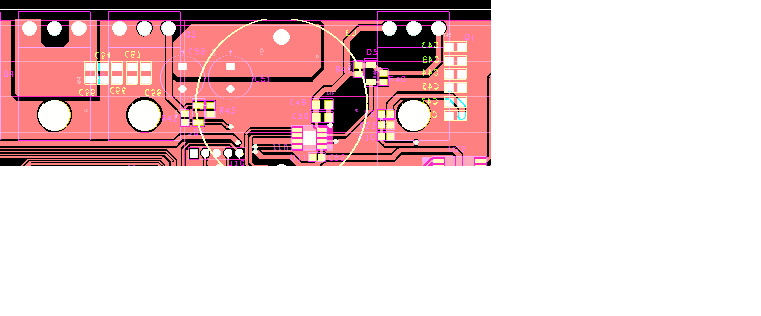
    Lastly, please take a look at the layout for the driver IC. Is the power pad connected through wide copper traces to the PCB ground plane for heat sinking? Feel free to share that section of the layout for review.

    Please let me know the items above and/or any other updates you may have so we can continue working on this debug.

    - Daniel

  • Dear Daniel,

    please find reply below for your queries.

    1. Is the FET at the output meant to conduct via its body diode, to a load? 

    Yes.


    2. However, you mentioned a high current when this FET is installed. Please confirm: the same behavior is not observed if instead of the FET, there is a direct connection (short) to the load.
    Its same with other MOSFET's too,. Will test and revert for current when output is shorted.


    3. Does anything change in the running conditions between startup time and when the device fails? I notice you mentioned a long run -- how long a running time is that? Does the device get hotter and hotter over time, or does it get hot suddenly just before failure?

    In Our system its mainly for charging battery. So on depending on battery status. It gradually gets hottet and hotter some times it just blows off.


    4. Other places I would look are the VDD and HB supplies. When you check with a scope, are they remaining steady, or do they fluctuate? About 300mV ripples seen when buck operates.


    5.The HB supply needs to be refreshed periodically by switching on the low-side FET.

    please elaborate query to advise


    6.Lastly, please take a look at the layout for the driver IC. Is the power pad connected through wide copper traces to the PCB ground plane for heat sinking? Please share section of the layout for review.

    Will soon share the layout.

    Rgds,

    Aravind.

  • Dear Sir,

    Also charger buck layout attached for your kind reference.

    Aravind.

  • Hi Arvind,

    I am Systems Engineer in Drivers group.
    Have you submitted any of the failed parts for FA to TI?
    If not, I would recommend to do so.
    Does power MOSFET fail when driver fails?
    Is this system in production and deployed in the field or this is prototype?
    Can you tell us how many drivers have been used and how many of them failed?
    Have all of them failed in the same way?
    The operation of power stage should not impact the driver power
    loss. Even if you short circuit the output, the duty cycle might change, but I believe you would have maximum and minimum duty cycle clamp.
    If possible take a waveform of HO, HB(with reference to HS using differential probe), LO and VDD when the output is short circuited or loaded very heavily.
    I am sure Daniel have already looked into this, but let me also take a look into possible power loss in the driver.
    You can properly thermocouple the driver and the board area around it. By doing so we can compare theoretical temperature rise and actual temperature rise.
    Let us keep investigate.

    Regards,
    Ritesh
  • Hi Arvind,

    Yes we did roughly calculated the power loss and it was not much.
    Let us look at the waveform and see if we can find something.

    Regards,
    Ritesh
  • Dear Ritesh,Daniel,

    please find below needed replies, please advise your valuable feedback.

    Does power MOSFET fail when driver fails?
    Yes mostly high side fet fails, sometimes even low side.

    Is this system in field or this is prototype?
    At present it is in building stage and worked on in lab

    Can you tell us how many drivers have been used and how many of them failed?
    Many drivers, may be more than 25 !! on various boards have failed. We have only two boards which work properly. Similarly about 30 MOSFETs might have failed by now.

    Have all of them failed in the same way?
    Yes. They get hot and pop off.

    The operation of power stage should not impact the driver power
    loss. Even if you short circuit the output, the duty cycle might change, but I believe you would have maximum and minimum duty cycle clamp.
    Ya we have duty cycle limit.

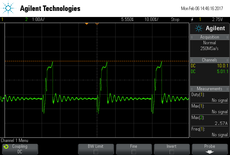
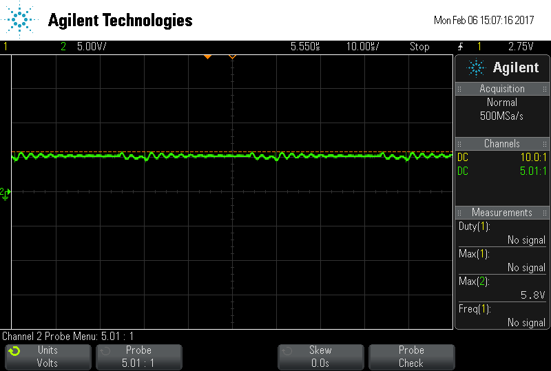
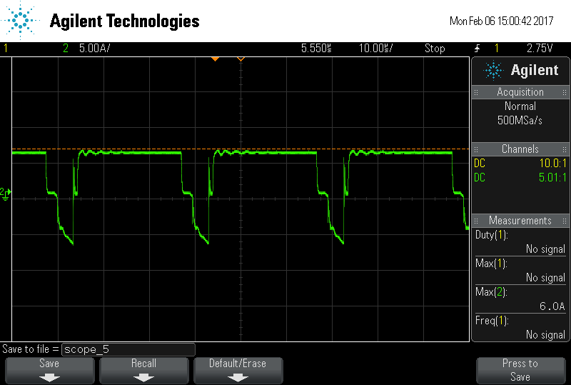
    Necessary waveforms attached for reference.

  • Hi Arvind,

    Thanks for the waveform, but I could not see the label for each waveform and therefore I cannot say what is what.

    If you never had an instance where only driver failed, then there is a high probability that the power MOSFET fails first and that takes the driver along with it.

    At this point, we should try process of elimination.

    One idea is that you test driver by itself, with capacitive load (based on gate charge of the FET being used) on its output and see if driver fails?

    For this test you can keep all other test conditions the same, such as frequency, duty cycle, ambient temp, the board, etc...

    I hope we can start eliminating possibilities.

    If there is a way to reproduce the failure in a controlled way, we might want to take waveforms of various signals before failure happens. We can shut-off the system before it fails.

    Also, please provide the label for the waveforms.

    Regards,

    Ritesh

  •     Dear Ritesh,

    please find attached waveforms with labelling.

    Aravind.

  • Hi Arvind,

    The waveforms do not look correct.

    For example the scale for LO and VDD is shown as 5A/div, unless I am missing something.

    This should be V/div.

    I also see some negative amplitude for LO. LO must not go negative for such a long time and so much amplitude.

    I also see that the VDD is dipping. It should not be like that. VDD must be constant.

    HB seem to be 5V. Is that what you expect?

    Did you measure HB with respect to HS with differential probe?

    HO also shows A/div. It should be V/div.

    Either this device is already damaged or there is something major wrong on the board.

    As I suggested earlier, would you please do the testing with just the driver (and associated bias) with capacitive load on it.

    I believe there is something else in the board wrong.

    If you wish, you can share the complete system schematic to see if there is anything wrong.

    Please let me know about the waveforms so that we can discuss this further.

    Thanks and regards,

    Ritesh

  • Dear Ritesh,

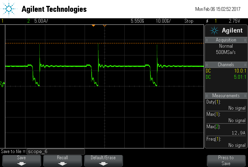
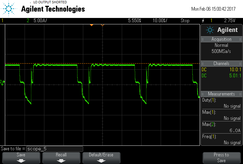
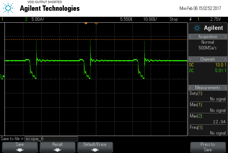
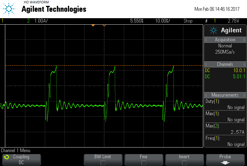
    please find attached waveforms,  please review and advise.WAVEFORMS.docx 

    Yellow- Voltage waveforms

    Green - Load current

    Rgds,

    Aravind.

  • Hi Arvind,

    There is still some inconsistency or problems with the waveforms.

    For example, first waveform shows some pulse skipping, which should not be the case.

    Second waveform says that it is with reference to HS but looking at the V/dv, it seems that it is with reference to ground.

    It also seems that there is lot of noise on the board. The HS plane should not be over any plane in the board.

    The driver need to be as close to the power MOSFET as possible, specifically the output loop lengths (LO to VSS and HO to HS) need to be as small as possible.

    It also appears from first 3 waveforms that there is some cross conduction, LO is ON when HO is ON.

    This might be causing overheating and eventually failure.

    To fix this, layout need to be improved. May be some input filtering might also help.

    When gate resistor is changed to 1k, I do not know why high side gate voltage is different at different load. Vgs is 5V at light load but goes to 12V at 15A.

    It should not be that way.

    My recommendation is to increase VDD capacitor to let us say 10uF and increase HB capacitor to 1uF and observe the behavior.

    It is also recommended to place high frequency filtering cap for both VDD and HB.

    I also recommend you get some new samples of UCC27201A to rule out bad lot.

    If your customer can ship board to me, I can try to look into it in my lab.

    May be it is a good idea to do a webex and conference call with customer if possible.

    Regards,

    Ritesh