A related question is a question created from another question. When the related question is created, it will be automatically linked to the original question.
If you have a related question, please click the "Ask a related question" button in the top right corner. The newly created question will be automatically linked to this question.
Hi John,
here i add more details.
The picture is 3 dc2dc input connected to 50v power supply LAB and their output connected to servos , 2 servo to 1 output.
The LAB power supply is on always.When we turn on and off and on ,often the enable pin demage of tps40170.
There is addition 2 dc2dc connected to iput voltage 50v (the same vin) ,but their outputs connected to computer and other loads that are not servo.
the enable signals are all connected toghther.
4 dc2dc base on tps40170 the last base on tps54560.
I know ,the load to dc2dc base 40170 is servo and we operating the servo after few hours the tps40170. Demage in enable pin or current limit what can cause to blow up thr chip? Pls send me ideas.
I agree with John that 4V should not damage the EN input. Since this is a high impedance input you might experiment with placing a series resistor (2.2k?) on the enable input line. This may allow you to debug the issue and prevent input damage so that you can get the system running. Maybe there is an issue with ground potential difference between the enable source and the controller, particularly during startup.
2 boards their tps40170 were demage,after 2 days of work.
First board the enable pin demag at tps40170.
Second board was very hot near current limit pin and after loading it with resistor of 6 ohm it blow up at pins 18,19,
The board connected to 2 servos use as load .
The borad first got 50v input when enable pin is in ov,then we switch on and off and on supply pwm to the servos after while tps40170. Blow up,what is the problem?
The board dc2dc with 40170 is connected to 2 servo.
1. first apply 50v to his input ,when the tps40170 is disable by enable=0v,no 7.4v at output.
2. we enable the tps40170 by put the 2n7002 at cutoff ,as result enable= 4v.
3. apply PWM to move the servos.
5.stop to apply PWM to servos.
6.disable tps40170 (enable pin is grounded).
7.then turn on the tps40170 by put the 2n7002 at cutoff ,as result enable= 4v(divider voltage).
doing 1-7 during 10 hours ,as a result the tps40170 demage.
The current one servo take from dc2dc is about 6A for short time msec.
If the Enable pin is damaged it is likely over voltage damaging the pin. However, you mentioned that pin 18 and 19 are damaged? Are pins 18 and 19 damaged in addition to the Enable pin? Or is pins 18 and 19 damaged and the Enable pin is not? Also, you mentioned that there is some overheating present at the current limit pin?
I think we should take a step back and determine if the controller is working correctly first. Can you let me know what your efficiency is running at full load? Also can you let me know how hot the components are getting, is it possible to get a temp measurement of the board? Also can you show me a scope plot of the Switch node, High side gate drive, and Low side gate drive while running at full load, in steady state, or at a load where you are seeing damage? I would like to first make sure that the steady state performance of the converter is good. After, we can then look at some waveforms during start up/Restart conditions?
f the Enable pin is damaged it is likely over voltage damaging the pin. However, you mentioned that pin 18 and 19 are damaged? Are pins 18 and 19 damaged in addition to the Enable pin? Or is pins 18 and 19 damaged and the Enable pin is not? Also, you mentioned that there is some overheating present at the current limit pin?
*answer:i have 2 boards that tps40170 fail:
the first board fail because pin enable demage.
the second board fail,because the TVS( SMBJ51A at input) not solder well and current limit pin was over heating.in the second board the pin enable was not demage.
I think we should take a step back and determine if the controller is working correctly first. Can you let me know what your efficiency is running at full load? Also can you let me know how hot the components are getting, is it possible to get a temp measurement of the board?
*answer:the tps40170 go to 80 C without load.
with load it is 80 t0 82 C.
load current is 6A for short time when the servo move.0A when the servo not move.
we make same change ,but i am not sure that it solves the problem.
the change we made we short D5 and replace R2 FROM 0 OHM TO 2.2 OHM.
R2 =2.2 ohm reduce the pulse in SW signal.
VIN rise to 61.4v for short time when the servo move because of that D5 was shorted .
after shorting D5 VIN was stable.
I just realized we had a conference together earlier this week and I had discussed how to calculate the IC Temp from the total Gate charge of the top and bottom FETs.
If we assume that the TVS is correctly soldered, then the issue is with the EN failing? At least for now? I would assume, first, that this is related to the voltage exceeding the abs max for some reason? I believe I had suggested further modification to the Resistor divider network to reduce the voltage seen at the Enable pin, while still satisfying the Enable threshold to turn on. Have you tried this and retested?
Increasing R2 will certainly slow down turn on time of the high Side MOSFET and certainly reduce voltage ringing on the Switch node. You will have to retest to be certain that this fixes your issue?
not yet ,because i think the problem is the servo not has back EMF diode.
Increasing R2 will certainly slow down turn on time of the high Side MOSFET and certainly reduce voltage ringing on the Switch node. You will have to retest to be certain that this fixes your issue? i agree.
what protection you think i have to put for inductor or coil load?
Because the load is a servo motor perhaps as you shut off either the motor or the TPS40170 the stored energy in the drive back feeds into the regulator output. There are two possible events that might be the issue.
1) There is a chance that when you turn off the regulator with the enable input line that the stored energy in the servo discharges, commutates, and draws the output voltage of the regulator stage below ground for a short period of time. Pulling any pin of an IC below ground while it has Vin applied can trigger any number of issues, none of them good. Try installing a reverse biased Schottky diode across the supply output so that if the output is pulled below ground that the level is clamped at one Schottky forward voltage drop externally and this should protect the controller IC.
2) Any synchronous buck that allows reverse inductor current can process power in the reverse direction and become a synchronous boost. This would occur if the output voltage was raised above its programmed regulation value. Events of this type can cause the regulator input voltage to increase, possibly to a level that exceeds the rating of the device. As an experiment, you might try a series diode from the regulator output to the servo supply input. This would prevent the supply from ever running in synchronous boost mode because the diode prevents reverse current.
As mentioned, I think the issue is relating to a voltage presented to the Enable pin that exceeds the abs max. Reducing the voltage presented to this pin, would help determine if this is the cause of the failure.
If you believe there is a voltage spike at the load that is feeding back to the input, the only option I can think of is to use a TVS. It looks like you already have a TVS in place and the TVS appears to be working because without it, you experienced a failure. The other Option that I can think of to increase robustness is to use an IC that has a higher Abs max voltage rating at the input?
I have tvs diode smcj15a at the output is it doing something you said above?
Another think if tps40170 is very hot about 80c do you think we have to remove the heat with heatsink or be sure that thermal shut down protect the chip tps40170?
Clearly the voltage from the output is feeding to the input though the Body Diode of the Top Side FET, as Alan alluded to in his post. And as such, in my comment, I was referring to the input TVS. I looked up the SMBJ51A and this is not going to protect the IC, as the max breakdown voltage for this device is 62.7V which violates the abs max for the TPS40170.
I believe this is your issue and unless you can control the voltage that is feeding back from your load, to be below the Abs Max of the Device and its pins, you will be at risk of device failure.
Regarding the IC temp, as previously discussed on the conference call at Vin >50V continuous, your losses are greater than 0.5W and could be much more if the Gate Charge of the FETs or more than the published typical numbers. As recommended previously, please do one or more of the following, increase the DAP area, decrease switching frequency, decrease the total gate charge for top and bottom MOSFET, or somehow reliably attached a heatsink to the IC??
For case 1. a TVS rated much lower than the input voltage abs max ratings should protect the device provided the energy in the voltage spike does not exceed the ratings of the TVS.
For case 2. Please post a schemetic?
For Case 3. Again depends on the amount of energy in the voltage spike
For 3 what is the formula between the energy spike and the CAP output value in the buck?PLS explain how Increase CAP value will protect the buck from spikes?how can i be sure that the spike will not came to the input or will demage the tps40170?
Can spike turn off the buck converter despite we had power absorbed device in parallel to 2 servo that use as load to the buck?
PLS tell me what are the reasons colud be to turn off the buck?
I think that meauring the current in the inductor is worth while, to see if the Sync buck is operating as a boost in the reverse direction when the voltage spike on the output is present. Please can you place a current probe inline with the inductor and measure the inductor current and the Switch voltage when the Servo turns off?
How i can measure the current?my probe current bandwidth. 100kHz. And it is clamp current that diffcault to clamp to inductor is there another. Way?i see when i rotate the servo fast the input voltage became about 62v,.because the servo supply positive voltage to the output buck.
i think the output CAP and the power absorb Device operate both. so if i put at the ouput series diode ,the buck be only buck in one direction or increase. The output buck CAP. To 400uf,i do not know if it solve the problem.
PLS. Advice what is better soultion ?
PLS. Answer. To my questions. Before
If you do not have a current probe that can measure the current, I suggest getting a series resistor (current sense, low ohms) and measure the voltage differentially across the resistor. Without understanding what is happening, I am not sure I can detemine the root cause of your issues?
You should be able to use the clamp on current probe. Simply lift one end of the inductor from the PCB and install a short length of wire from the lifted terminal of the inductor to the PCB pad. It is best to use the output side of the inductor, not the switching side.
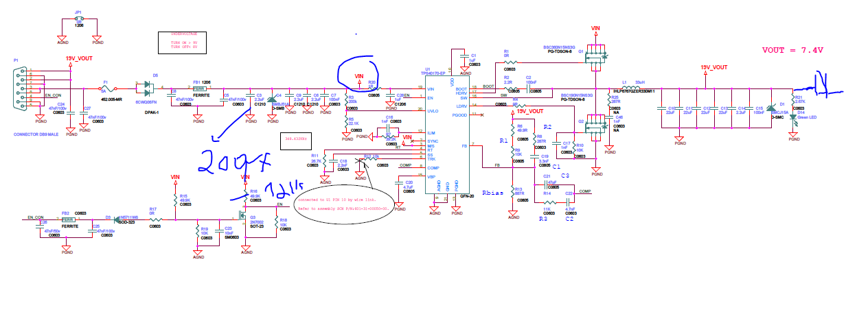
I finally see the issue that damages the enable input. The enable divider is R15 and R18. 49.9k and 10k respectively. These divide Vin by 10/(49.9+10) = 1/6.
In the case where your servo winds down and pushes Vout (and hence Vin) up to 62V will result in 62/6 = 10.33V on Enable. This exceeds the 8.8V rating of Enable Input (and is also the ABS max rating of the TPS40170!). If you can't change the UVLO points of 8V and 9V then place a small 5.6, 6.2, or 7.5V zener across R18.
Since this supply is set for 19V output you should really have a UVLO level that is notably higher than 19V such as 25 or 30V considering this is a 50V input power bus. The 8V and 9V UVLO thresholds as drawn would be appropriate for a 5V or 3.3V output regulator and not for a 19V output application.
It the servo is truly reflecting energy back into the 19V output to the degree that it is pumped up to 62V I expect additional problems will occur in this system. You might consider a voltage mode controller that will allow reverse inductor current, that will operate backwards as a synchronous boost. This will tame the voltage excursions on the 19V output rail and take the reflected power out of the servo and return it to the source. You will need Schottky diodes across both top and bottom MOSFETS in that approach.
i add shunt resistor in series to L1 and i measure the current ,i did not find diffrent in the wavefrom with servo and without,but i find that when i add series diode between dc2dc output to servo the VIN stop to increaes to 62v it was stable 50v and the PWM peak stop to increase .
I know according to data sheet tps40170 that when it in OCP after the couter is value=7 it turn off the tps40170 why is it not trying to wake up again ?How can i remove OCP ?