This thread has been locked.

If you have a related question, please click the "Ask a related question" button in the top right corner. The newly created question will be automatically linked to this question.

WEBENCH® Tools/TPS40304: Failure in Cold Temperature (could be OCP-Overcurrent protection)?

Part Number: TPS40304
Other Parts Discussed in Thread: CSD16321Q5

Tool/software: WEBENCH® Design Tools

Hi,

Having rather rare issues in cold temperture (-40c) with the tps40304 design.

Also in is are the MOSFET (CSD16321Q5) as the lower and upper FETs.

 The output voltage (1.0v)is dropping (few second after power up). Input voltage (3.3v) is stable. probbing the SW pin, and pulses are ceasing (No pulse signals).

It looks as if the VRM is shutting. Enable pin is "ON".

I tried to increase the OC resistor. Works (failure not duplicated) on one board, failing on another board.

I have noticed that both contorller and MOSFET datasheets we updated in 2016 (the design was based on older datasheets).

How can i confirm i have an OCP condition? i cannot measure the output current , with the current setup (theoretical analysis shows that i am not in over current issue).

Could there be other reason for VRM shutdown?

P.S. On the first failiure occurence, the tps40304 and mosfet were replaced.  failure was not reproducible after that. (and as i said this is a rare failure).

Thanks,

  • Hi, Oded,

    To check whether it's OCP shut down, you can probe either the EN/SS pin or Vout after shut down. If you observed hiccup behavior on Vout and the Vout restart ramp are four or five dummy soft-start timeouts apart, OCP shut down can be confirmed. Please check page 11 of the datasheet about the hiccup response.

    As temperature goes low, the internal current source used to set OCP threshold decreases while the Rds_on of FET also decreases, it's possible the actual OCP threshold becomes lower.

    If increasing the OCP programming resistor can solve the issue, then that could be the effective solution.

    Thanks.
  • Dear Ray,

    Thanks for your response.

    i will try to duplicate the failure, probe the output voltage and look for the hiccup condition...

    meanwhile, my calculation of the OC resistor, after taking in account the Iocset as 8uA (value @-40c),  and even not decreasing the Rds value, i still see that  for the maximal value of current i considered (Max 17A, although actual consumption is not more than 12A) the Roc is equal to 4.5Kohm (the original value is 4.7Kohm).

    Can you please double check my Roc value?

    Thanks,

    Oded

  • Hi, Oded,

    You calculation is OK. From the equation, 4.7k should be sufficient for more than 25A load, given 2.5m ohm Rds_on and 8uA Ioc.

    Thanks.
  • Dear Ray,

    You wrote:

    "If increasing the OCP programming resistor can solve the issue, then that could be the effective solution."

    But if my calaultion of the Roc is ok, i don't understand what is the root cause.

    Please advise,

    Oded

  • Dear Ray,

    yet another question.

    1. Does suppling the TPS40304 with 3.3v can effect the OCP function in cold temp?

    2. With regarding the MOSFET, what is the maximum Rds_on while the VGS is 2.45v (3.25-0.8)?  is this MOSFET suitable for design which powers the tps40304 from 3.3v?  Does the 6v internal Regulator is operated in this case?

    3. What is the TOP MOSFET gate voltage drive when opeating from 3.3v VDD?

    Thanks,

    Oded

  • Hi, Oded,

    1. Supplying TPS40304 with 3.3V may impact the OCP threshold even at room temperature. The BP voltage would follow VIN voltage if VIN is lower than 6.5V. Since the driving voltage for main FETs are based on BP voltage, with lower driving voltage, the Rds_on can be higher, which eventually would impact the OCP threshold.

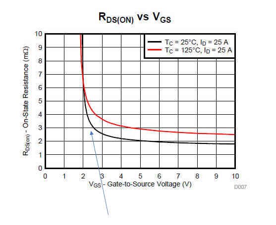
    2. From datasheet of CSD16321Q5, the Rdson is about 5.4m ohm when Vgs is 3V. So the 5.4m ohm Rdson should be considered when calculating the OCP.

    3. I think the gate driving voltage would be same as BP voltage. Given the 3.3V input, probably BP voltage is about 3.2V.

    Thanks.

  • Dear Ray,

    We have repeated the webench simulation.

    We have simulated the VRM both in -40c and in+50c.

    simulation shows that in -40c we need to set the Roc to 7.5K ohm.

    however, We still try to understand the calcualtion.

    1. Can you please help explain how the Roc is calculated with the given datasheet formula?

    2. Do you have any information regarding the Vocset@-40? datasheet specify the valueonly  @25c.

    parameters used for the simulation

    vin=3.1v to 3.4v

    vout = 1.0v

    Iout=17A

    Temp=-40c

    TPS40304

    Thanks,

    Oded

  • Oded,

    I am responsible for TPS40304 part support and will help figure this out. First of all can you share the schematic.

    1) When you find a board that has an issue please remove R11, figure 14 of the datasheet and restart power to the board. See if the issue still exists. If the issue goes away then we can narrow down to the OCP setting of the Low side FET. If the issue persists then we have found the root cause to be the fixed high side OCP limit.

    VOCH OC threshold for high-side FET TJ = 25°C 360 450 580 mV

    These numbers are at 25C and the temp coefficient is 3000ppm/C.

    Regards,

    Mathew


  • Oded,
    In your schematic dId you short the Vdd pin and BP pin (pin 1 and 10). There is an internal regulator between Vdd and BP and the dropout voltage of this regulator may also be affecting the circuit since you have a low VIN. Can you also try shorting the pin 1 and 10 on the bord you have problem.

    Regards,
    Mathew
  • Hi Mathew,

    Thanks for your response.

    regarding your question,

    No, i have not shorted VDD and BP pin. BP pin connected to a bypass capacitor (1uF) to Ground.

    Is there a recomandation for doing so in the datasheet? pls point me to it. (btw, it was not in the webench simulatio as well)

    I will try to do so.

    Thanks,

    Oded

  • Oded,
    I have ordered the board and the same fet you are using so can try to replicate here.

    Regards,
    Mathew
  • Oded,

    There is no recommendation in the datasheet but its okay for testing. It looks like you are running out of headroom for the  fet Vgs since you have a low Vin. By shorting the VDD and BP pin you are removing the drop of internal regulator. I have got the fets in hand and should have the EVM in 1-2 days and will test this at -40C.

  • Dear Mathew,

    Appriciate your help very much.

    Can you please also refer to my question asked before.

    We have preformed a webench simulation @ -40c, and got that thr Roc should be 7.5K.

    We have also check this solution on a failing board in a temperature chamber, and we have reproduced the issue.

    Can you help understand how can calculate the same value (7.5K) from the furmula given in the datasheet? this would help us in convincing our client in the proposed change.

    Can you also clarify the Vocset value in -40c?

    Thank you very much,

    Oded


  • Hello Mathew,

    Could you determine, how exactly the current of high side FET is being sensed?

    Would it be possible to connect VDD to higher voltage (for instance 5V) where the input voltage to the power stage would be lower (3.3V)?

    Regards,

    Alon Blumenfeld

  • I got the schematic you are using however please confirm the output capacitor values and type. In plugging in your circuiit values see very low phase margin. The schematic I got shows 2 x 100uF,10V caps on the output. Once you confirm values I will try to replicate in lab over temp.
    Regards,
    Mathew
  • Dear mathew,

    Thanks for yor response,

    schematic show s only 2 capacitors, 1210X107K100SNT, in the VRM output.

    However there are additional capacitors near load (keep in mind that the load is only 7-8 cm away):

    6 x 100uF.

    41 x 100nF

  • Oded,

    Thats okay then. I tested on the evm and current limit equation is matching for Vin>5V with the particular fets you are using. When Vin<5V the max output current is reduced quite a bit. Am modifying to your values now and will test.

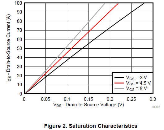
    There is one curve on the fet datasheet which is interesting .

  • Based on the above curve for the CSD16321Q5 at Vgs=3V, @20A, Vds>50mV. If you are setting 4.7k for Rocset and 10uA current you are already at 47mV so quite easy to run into problems. For an application at 3.3Vin I think your fets are undersized and you need to use bigger fets unless you set a high value for the Rocset. I think this is the root cause.

    Regards,
    Mathew
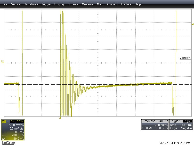
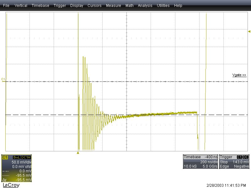
  • Switch node waveform at Vin=5V, 80mV drop at 20A transalates to 4mohm Rdson approx

    Switch node waveform at Vin=3.3V, 95mV drop at 20A transalates to 5mohm Rdson approx

    So there are 2 factors affecting current limit tripping, one is the higher Rdson as the Vin is lowered to 3.3V , second is the switch node ringing which can also cause tripping.

    Some OCP measurements with your circuit values at Vin=3.3V:  85C 23A, 25C 23A, -40C 18A

    Vin=5V; 25C 29A, -40C 30A

    By adding a snubber from SW pin to GND, 2.2ohms and 1nF the ringing reduced

    OCP measurment at Vin=3.3V, 25C 29A, -40C 23A

    Uisng CSD16321Q5 fets and operating down to 3.3V  Roc needs to be set higher and ringing mitigation technigues need to be considered, snubber, slowing down gate drive signal with resistors can be considered unless you are changing to lower Rdson fets at 3.3 Vgs.

    Regards,

    Mathew