This thread has been locked.

If you have a related question, please click the "Ask a related question" button in the top right corner. The newly created question will be automatically linked to this question.

TPS54229: The chip is damaged when the output short

Part Number: TPS54229

Dears,

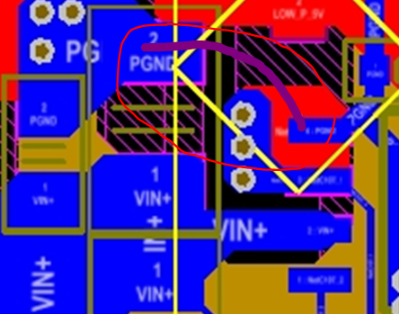
I tested the TPS54229, the circuit is work stable, but the chip continues some minutes will be burned  when I short the output. I found the chip is strict requirement the PCB layout, is it related with the chip destroyed? Thanks very much.

Best regards!

Jacking Jin

  • Dears,

    Could you kindly give me some suggestion? Why my chip is burned when I short the output? Is it realted with PCB Layout or the chip can't support the function? And Could you help me simple explain what's the D-cap2 technology? Waiting your reply!

    Best regards!

    Jacking Jin

  • Hi Jacking,
    Could you please upload your schematic and layout for review?
    First let me simply say someting about D-CAP, D-cap is by detecting Vout ripple to determine when turn on High-side mosfet, when VouT ripple goes down lower to the VFB, drvier will turn on Hight mosfet to charge L to make Vout go high, the on-time of High mosfet is determined by VOUT/VIN, after the fixed on-time, High mosfet will turn-off, which will cause Vout goes down to VFB again,.....repeat the cycle..
    Dcap2 is upgrade of D-CAP, just integrate ripple injection function, so this topology can support Lower ESR cap, such as MLCC, which can make Vout ripple very smaller.
    and also you can read the "detaied description" at page7 in TPS54229 DS.
  • Dear Yuchang,

    Thanks for your detail explain and reply!

    Attachment is the TPS54229's SCH and wave, please help check it, thanks!

    Best regards!

    Jacking JinTPS54229 SCH.docx

  • Hi Jacking,

    Thanks for reaching out to us. Before we know what is happening to IC, I would like to know more info here:

    1) For the short test, is it directly short on output cap? Did you capture any waveform during the short?

    2) Could you show me the specs of the inductor you use? Inductor could be saturated during short when wrong selected. 

    3) I found a big 220UF electrolytic cap used at output, could you remove that cap and test short to see whether the IC will damage? 

    4) For the layout, could you show the trace or polygon connecting from input cap to GND pin( as shown below)? The trace should be on the top layer and directly connected as short and wide as possible. 

    5) Did you check whether the IC is soldered well when you test short output? We found failure before when not soldering well on PGD pad. 

    Let's have a further discuss when I got these info. 

    Best,

    Anthony

  • Dear Anthony,

    Thanks for your reply! About your question as below,

    1) For the short test, is it directly short on output cap? Did you capture any waveform during the short?

    Yes, direct short the cap, I'm regret that I haven't save the wave, I will resave it later.

    2) Could you show me the specs of the inductor you use? Inductor could be saturated during short when wrong selected. 

    4.7uH/6A(I will test the inductor current waveform later)

    3) I found a big 220UF electrolytic cap used at output, could you remove that cap and test short to see whether the IC will damage? 

    I will try to testing it . I want to know that I remove 220uF cap whether influence the output ripple .

    4) For the layout, could you show the trace or polygon connecting from input cap to GND pin( as shown below)? The trace should be on the top layer and directly connected as short and wide as possible. 

    OK, thanks for your suggestion, and what about other layout? Please kindly give some suggestion.

    5) Did you check whether the IC is soldered well when you test short output? We found failure before when not soldering well on PGD pad. 

    I had check the solder is no problem.

    Best regards!

    Jacking Jin

  • Hi Jacking,

    For DCAP2 devices, big output cap could worsen the loop response and lead to poor transient performance. So I would like you to remove it and try whether there will be improvement. 

    For the layout, I got only one concern on the input cap to GND trace. Found no more at present.

    Best,

    Anthony

  • Dear Anthony,

    OK, I will try to do it.

    If  we remove the big output CAP how can we maintain the power supply of the down-stream product. Looking forward to your suggestions, thanks!

    Best regards!

    Jacking Jin

  • Hi Jacking,

    From our previous experience, 22UF  to 68UF is good enough for the output and downstream. DCAP2 has a superior load transient performance and it could support the downstream power without issue. However, too big output cap could make the transient worse and interference with the soft start process. 

    Best,

    Anthony

  • Dear Anthony,

    Noted! Thanks for your great help!

    Best,

    Jacking