This thread has been locked.

If you have a related question, please click the "Ask a related question" button in the top right corner. The newly created question will be automatically linked to this question.

BQ24266: Reducing BQ24266 output voltage to 4V from 4.2V and reduce heat dissipation for GSM application - VALTRACK-V2 GPRS tracker

Part Number: BQ24266
Other Parts Discussed in Thread: BQ24261M

Hi, 
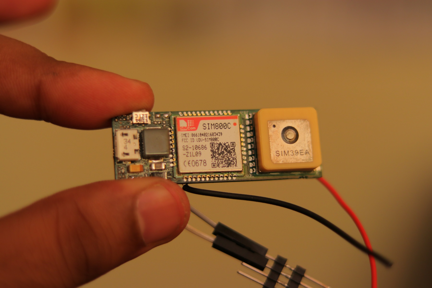
I  am using BQ24266 after recommendation from Michael from TI asia team for my requirement for personal/vehicle tracker VALTRACK-V2 gps tracker application to support vehicle input voltage of 12V and supply load and charge internal battery at a time. The design is ready and PCB is assembled and charger is working but the output voltage on SW pin goes from 4.2 to 4.28 volts when charger is connected . 4.3V is  the maximum voltage the SIM800 GSM module can take. And it starts giving over voltage warning and gets warm. Even the BQ24266 is getting hot when charging.

Is there any way i can limit the voltage to 4.0V at output ? 

How can i calculate the charge current. I am not able to understand the Kieset value mentioned in datasheet. ?

Can BQ24266 run fine in long term inside vehicle supplying power to load and keeping battery charged for emergency purposes. ?

Is this heat normal when running at 12V input, Do i need a heat sink? 

The Inductor parts recommended in EVM datasheet were out of stock so i chose this inductor, Please check if its suitable.

I have tried chaning the IUSB lines to all possible combinations but the BQ24266 keeps getting hot.

The PCB is a 6 layer board and its cramped up. 

ASPI-7318-1R5M-T

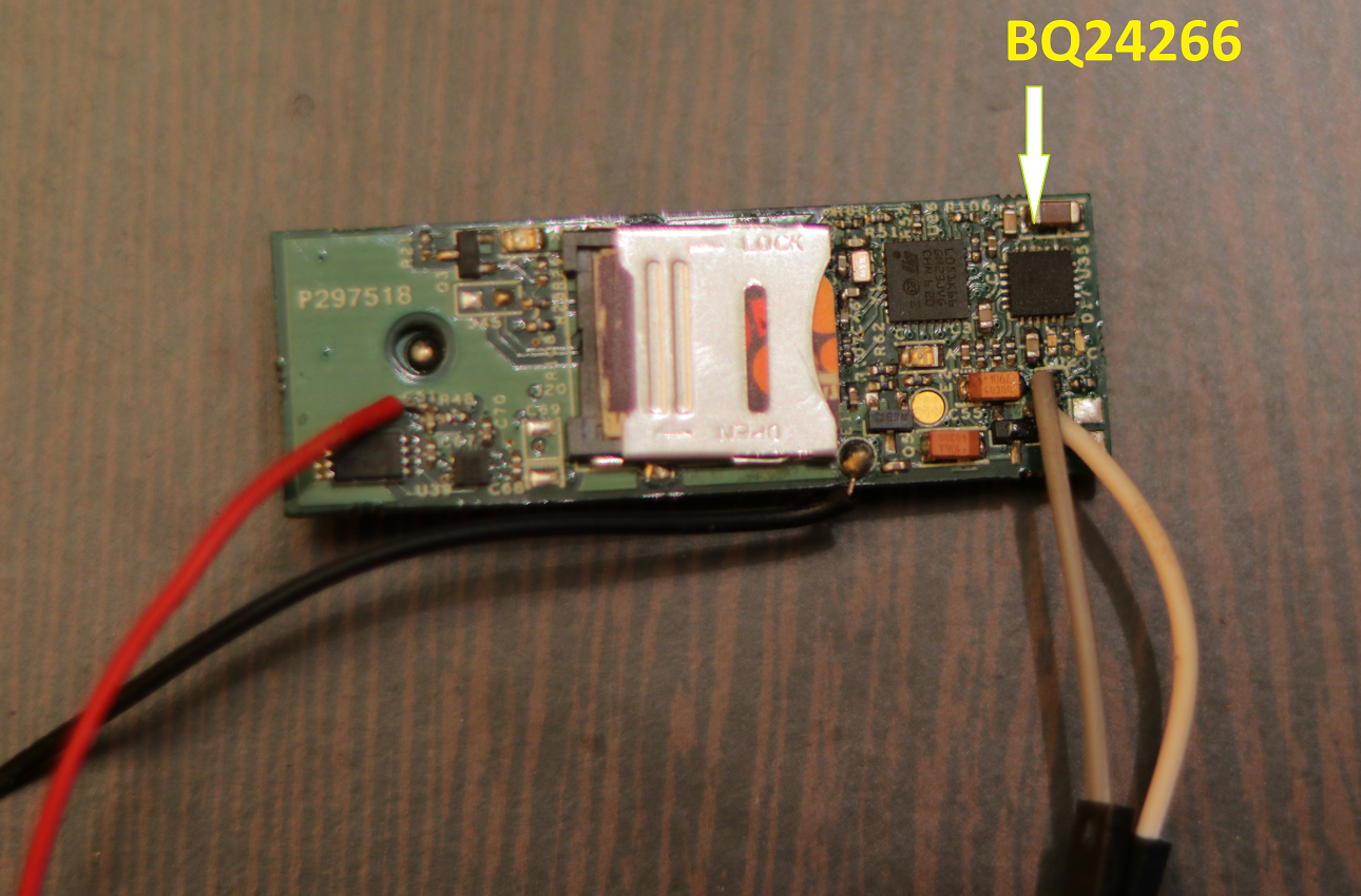
Attaching the schematic and the PCB images of front and bottom for reference

  • Ravi,

    From schematic review, please increase capacitance on DRV to 2.2uF. Inductor looks okay.

    Regarding "Is there any way i can limit the voltage to 4.0V at output ?":

    The battery regulation is fixed to 4.20V, with SYS being slightly above that, in order to fully charge a typical LiIon battery. Can you add a linear regulator or buck dc/dc converter following SYS output. If you are concerned about switching ripple peaks on SYS, you can increase the capacitance on SYS and/or the inductance from 1.5uH to 2.2uH.

    Regarding "How can i calculate the charge current. I am not able to understand the Kieset value mentioned in datasheet. ?":

    The datasheet equation 2 has a typo. It should be ICHARGE = KISET/RISET = 1200(typ)/400 = 3A if not limited by the input current limit set by IUSBx pins or reduced because the load at SYS is pulling more current than input current limit can split between BAT and SYS.

    Regarding "Can BQ24266 run fine in long term inside vehicle supplying power to load and keeping battery charged for emergency purposes. ?":

    Yes

    Regarding "Is this heat normal when running at 12V input, Do i need a heat sink?":

    Is the powerpad on the bottom of the QFN packaged charger attached (or via'd) to a large ground pour/plane? Are other ICs using (possibly saturating) this plane with heat? The charger efficiency is lower at VIN=12V compared to VIN=5V so it will be hotter at 12V.

    Do you have I2C communication capability? If so, you could switch to the bq24261M which would allow you to change the VBATREG to a value below 4.2V.
  • Hi Jeff,

    Thank you for the quick response. :)

    I will increase the capacitance value on DRV, No problem.

    I could add a linear regulator but which part would you recommend for reducing 4.2V to 4V on VSYS while keeping the current >2A.

    Right now i am measuring voltage at VSYS to be 4.31V at 12V when charger is connected.

    The heating is happening at 5V and 12V as well. The heat generated is almost same at both voltage inputs. The power pad is connected with 2 vias to ground plane. The ground is poured on all layers with in addition to separate ground plane layer. The ground planes are shared by all devices including GSM module which also generates a mild amount of heat, but not more. Do you think it will saturate the ground plane? Any remedies for this?

    The typical value of KIESET will help, Thanks for that. So my input current is set to 3A right now because of 400 Ohms being used. ?

    I have I2C available on board, Are you saying that i can adjust the voltage that comes at VSYS which is provided to the system or the max voltage that the battery is charged to? I want reduction in the VSYS voltage in my schematic and want the battery to be fully charged?

    Is this chip BQ24261M fully pin compatible to my current part BQ24266? can i use it as drop in replacement?

    Also why there are two separate charge current limit settings, ISET and IUSB lines. How different are these? Dont they both limit the input charge current drawn from source? Please clarify.

  • Ravi,

    The SYS output voltage is a function of battery voltage. When V(BAT) > VMINSYS=3.5V, V(SYS) could be as high as V(BAT)*1.025. The charger will also provide at least VMINSYS=3.5V. So, even with an I2C part, you would have to lower the battery regulation voltage to prevent V(SYS)>4.0V. A linear regulator providing 2A from 4.2V to 4.0V would need to have very low dropout voltage (for when the battery is less than 4.0V) which is $$$. Also, it need to dissipate 400mV but most linear regulators designed to provide more than 1.5A will be in a big package, like HTSSOP or QFN. I suggest you use two >=1-A rated diodes in parallel between SYS and your output to more cost and size effectively drop the voltage. Alternatively/additionally, you could add a zener diode from SYS to GND, with a current limit resistor, that clamps the output voltage to the battery regulation voltage of 4.2V.

    I would expect the IC to be significantly hotter at VIN=12V vs VIN=5V, especially because at VIN=5V, the charger cannot provide 3A charge current at high battery voltages. The ground plane to which the power pad connects needs to be significantly larger than the power pad itself for optimal heat sinking.

    bq24261M is not pin to pin compatible with bq24266 because it has SCL and SDA I2C comm pins instead of IUSBx pins. bq24261M has a lower V(SYS) regulation point than bq24261M (+1.6% for261M vs 2.5% for 266).

    IUSBx lines (or the input current limit registers for 261M) are used to set the maximum input current that the charger is expected to draw from its power source. This is a safety measure used to prevent the power source from drooping/collapsing due to overcurrent. The input power (input voltage * input current) x efficiency is provided first to SYS output then to battery charge current. Typically, input current limit is set to provide both average system current and maximum battery charge current. If the input current is not high enough to provide both, the charger reduces battery current to prevent the system output from drooping and will enter supplement mode [V(BAT)=V(SYS)], where the battery helps to provide system current if necessary.