This thread has been locked.

If you have a related question, please click the "Ask a related question" button in the top right corner. The newly created question will be automatically linked to this question.

TPS650864: tps650864

Part Number: TPS650864
Other Parts Discussed in Thread: PMP12004-HE, MSP430G2121

Hi, I would want use PMIC TPS650864xx with Xilinx Zynq Ultrascale+ XCZU15EG but I found only version (TPS65086470RSKT) for Artix 7 that have OPT voltage value not compatible with my device. Where can I found a compatible device?

Thanks

  • Hi Giampietro,

    We have been working on several different TPS650864x OTP spins for Zynq Ultrascale+ but are still trying to determine which will go to production; it seems each application wants a different set of voltages.

    Are you able to provide your requirements? We expect the TPS6508640 settings (used in the PMP12004-HE TI Design) would be best for the ZU15 family, but we have seen a lot of variation. RTM schedule for that OTP is still TBD.

    One other option is to utilize a small MSP430 (like the MSP430G2121) to set all the voltages and sequence by I2C. This allows greater flexibility for opportunities where a custom OTP spin isn't cost effective.

  • Hi Kevin,
    my requirements are very similary to the PMP12004-HE, but on TI site I have only found Artix 7 version (TPS65086470) with OPT already programmed and not TPS6508640 version programmable with I2C.
    If I will find the correct version, when I power up the board, which is the output values befor configuring it with I2C?
    How can I keep the PMIC voltage output off while I program it?

    Thanks
  • Hi Giampietro,

    I wasn't very clear in previous explanation. For I2C setting, it is not writing a new one time programmable program but instead utilizing the registers when the device is ON. As long as all CTLx pins are low, the PMIC will not start up any of the regulators. One exception: LDOA1 is enabled by default on some OTPs. The TPS650860 has LDOA1 enabled by default, the TPS65086470 does not for example.

    After power up (when pre-programmed OTP is loaded), the voltage (VID) values can be changed and the rails enabled / disabled by I2C commands to create a sequence. This is true for any TPS65086xxx device. The TPS650860 is probably better suited because the LDOA1 is always on and provide power to the MSP430 (or other embedded controller) and has similar step size available (BUCK1-6 = 10 mV, 25 mV, 25 mV, 25 mV, 25 mV, 10 mV) to enable TPS6508640 settings but with BUCK1 and BUCK2 switched.

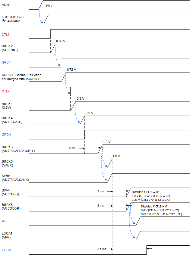
    If you think the exact TPS6508640 settings described in PMP12004-HE would work without any changes, let me know. We have historically found each customer needs at least 2-3 differences and so a custom OTP has been required where cost effective. The default voltages and sequence are shown in Figure 2.
  • Hi Kevin,
    ok I understand:
    1) Power up the board with CTLx pulled down, so the regulators are off
    2) LDOA1 power the embedded controller
    3) the embedded controller configure the PMIC with I2C
    4) the embedded controller drive high CTLx or enable regulators by I2C to create a sequence .

    It's correct?

    Thanks
  • Hi Giampietro,

    You are correct. Regarding step 4, enabling regulators by I2C should be used. The CTLx pin logic is stored in the OTP only so they should be kept low.

    Feel free to let me know if you have any questions.
  • Hi Kevin,
    sorry but what do you mean with "buck1 and buck2 switched"?

    Thanks
  • Hi Giampietro,

    For the PMP12004-HE design, they had BUCK1 = 3.3V and BUCK2 = 0.85V. For the TPS650860, BUCK1 step size = 10 mV, so range is 0.41 - 1.67 V and BUCK2 step size = 25 mV, so range is 1 V - 3.575 V. As a result, if using TPS650860 to implement PMP12004-HE, BUCK2 and BUCK1 need to be switched; namely BUCK1 = 0.85V and BUCK2 = 3.3 V.

    So a summary of the I2C program might be:

    i2cwrite(BUCK1_VID,0.85)

    i2cwrite(BUCK2_VID,3.3)

    i2cwrite(BUCK3_VID,1.2)

    [repeat for all used rails]

    i2cwrite(BUCK1_EN,1)

    i2cwrite(BUCK2_EN,1)

    i2cwrite(BUCK4_EN,1)

    [repeat for all used rails in sequence desired]

    In this example, I used BUCK1_VID to represent the 7 bits of the BUCK1_VID with a lookup table to convert 3.3V into 7 bits, but in reality it's probably easier to hard code something like i2cwrite(0x5E,0x20,0b01011010) for writing 0.85V into BUCK1CTRL register. Then for the I2C_RAIL_ENx registers just update the write sequentially (for example write 0b00000001 to enable BUCK1, then 0b00000011 to enable BUCK2 and keep BUCK1 enabled).

    I've attached the sample sequence we were considering for TPS6508640 OTP for your reference.