This thread has been locked.

If you have a related question, please click the "Ask a related question" button in the top right corner. The newly created question will be automatically linked to this question.

TPS22918-Q1: Questions for designing

Part Number: TPS22918-Q1
Other Parts Discussed in Thread: TPS22965-Q1

Hi,

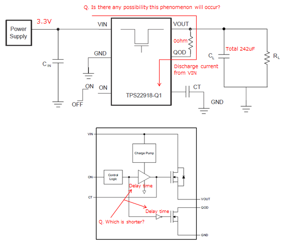
We got some questions from customer about TPS22918-Q1.
Could you help us?

[Question]
They are considering to design under following condition.

 Vin=3.3V
 Iout=1.842A
 Cout=22uF+220uF
 QOD=connected to Vout directly(not use external resistor)

- How much is the recommended range of QOD external resistor in their condition? They need external resistor because of output capacitor exceeds 200uF.
  So they want to know how to estimation.

- What does the maximum continuous switch current rating be related? If it is related only junction temperature, can the output current flow more than Imax at low thermal resistance board?
  Thermal resistance of thier board is 50C/W. On their board, can the output current flow 1.8A at Ta=95C?

- Which is shorter, the delay time of QOD or toff? If QOD will active untill FET still ON, discharge current flow from VIN. Is there any possibility this phenomenon occur? When they simulated by PSPICE, they found this phenomenon.

- They are considering QOD fall time. What can we estimate from equation 2? What does the Vcap stand for?
  We think fall time is CR-time constant. Can we estimate it from following equation?

   QOD Fall time = Rpd * Cout

- CT capacitor is connected to gate of FET. So they are thinking CT is related to tF and ON/OFF delay time.
  Does the CT capacitor be related to tF and ON/OFF delay time?

- Is there the variation data of Ron under the following condition?

   Vin=3.15 to 3.46V
   Iout=1.842A
   Ta=-30 to 95C

  They should estimate the variation of output voltage as accurately as possible. They don't need guarantee. They only use for reference.

Best Regards,
tateo

  • Hi Tateo,

    Based on all of your needs, it sounds like the TPS22965-Q1 may be a better device for your application. It has higher current carrying capabilities and can withstand the capacitive load of 242uF without a QOD resistor.

    To answer some of your questions:

    - How much is the recommended range of QOD external resistor in their condition? They need external resistor because of output capacitor exceeds 200uF.

    Is the customer looking to turn off the rail as quickly as possible? If they do not have a timing concern, I would recommend putting 100ohms or greater from VOUT to QOD.

    - What does the maximum continuous switch current rating be related? If it is related only junction temperature, can the output current flow more than Imax at low thermal resistance board?

    The maximum continuous switching current is based on both junction temperature and electromigration at specific temperatures. A lower thermal resistance board may help with increasing the amount of current the device can handle at a given ambient temperature, but it is difficult to say by how much without knowing how the board differs from the JEDEC standards.

    - Which is shorter, the delay time of QOD or toff? If QOD will active untill FET still ON, discharge current flow from VIN. Is there any possibility this phenomenon occur?

    QOD is not designed to activate until the FET is turned off, so VIN should not see this current draw when the device turns off.

    - They are considering QOD fall time. What can we estimate from equation 2? What does the Vcap stand for?
      We think fall time is CR-time constant. Can we estimate it from following equation?

       QOD Fall time = Rpd * Cout


    Vcap is the same as VOUT, it is the voltage on the output capacitor. Equation 2 can be used to estimate the time it takes for the output voltage to reach a certain amount. Simply put, it is an RC-constant, as you mentioned. I would use Equation 2 to estimate fall time instead of the equation you have above.

    - CT capacitor is connected to gate of FET. So they are thinking CT is related to tF and ON/OFF delay time.

    The CT capacitor has an effect on the delay time and rise time, but it has no effect on the fall time or turn off time of the device.

    - Is there the variation data of Ron under the following condition?

       Vin=3.15 to 3.46V
       Iout=1.842A
       Ta=-30 to 95C

    While we do not have this exact data on hand, the maximum 105C ambient numbers in the datasheet should give a good idea of the expected maximum on-resistance for the device.

    Thanks,

    Alek Kaknevicius

  • Hi, Thank you for your quick reply. Please check additional question.

    - They tried to estimate QOD fall time by equation (2). But the calculation result differs from Table 1. Please explain calculation example under following condition. What should we assign a value to "t"?

        Vout(Vcap)=3.3V
        CL=100uF
        Rqod=25ohm

    - They are considering about temperature rising. They estimated under the below.

        Iout=1.842A
        Ron=80mohm
        Ta max=95C
        θj-a=50C/W *on their board

        delta Tj = Iout^2 * Ron * θj-a
                      = 1.842^2 * 0.08 * 50
                      = 13.57C
        Tj = delta Tj + Ta max
            = 95 + 13.57
            = 108.57C

      So they are thinking the IC might be able to meet their requirement. Is there any concerns about thier estimation?

    Best Regards,
    tateo

  • Hi Tateo,

    - They tried to estimate QOD fall time by equation (2). But the calculation result differs from Table 1. Please explain calculation example under following condition. What should we assign a value to "t"?

    "t" is the amount of time it takes for the capacitor to discharge, and this is what the customer would be solving for. With an Rqod of 25ohms and CL of 100uF, it would take about 5.75ms to discharge the capacitor from VOUT to 10%. For this equation, Vcap is set to 10% of VIN, or 0.3V. Based on the values in the table, it looks like these calculations were done with a load of about 10ohms. However, I will confirm that this is the case.

    All that being said, with a load of 1.8A at 3.3V, there is an equivalent load resistance of about 1.833ohms on the output which will also affect the capacitor discharge. With this equivalent load resistance, it should only take about 420us for the capacitor to discharge down to 10%, assuming the load is on the whole time the capacitor is discharging.

    - They are considering about temperature rising. They estimated under the below.

        Iout=1.842A
        Ron=80mohm
        Ta max=95C
        θj-a=50C/W *on their board

        delta Tj = Iout^2 * Ron * θj-a
                      = 1.842^2 * 0.08 * 50
                      = 13.57C
        Tj = delta Tj + Ta max
            = 95 + 13.57
            = 108.57C

      So they are thinking the IC might be able to meet their requirement. Is there any concerns about thier estimation?


    On paper, the estimation looks good. My only concern is how the customer knows that their board is able to achieve a θj-a value of 50C/W. Have they done any testing to confirm this number? Did they use an IR camera to measure temperature on their board while the device was passing 1.8A?

    Thanks,

    Alek Kaknevicius

  • Thank you for your reply. Please let me know any update on equation (2). With regards to θj-a, I will discuss with customer.

    Best Regards,

    tateo