This thread has been locked.

If you have a related question, please click the "Ask a related question" button in the top right corner. The newly created question will be automatically linked to this question.

LM22674: V_IN Calculation & WEBENCH Simulation Issues

Part Number: LM22674
Other Parts Discussed in Thread: LM2267X-22680DESIGN-CALC,

Hi Team,

I have a customer who has a question about the formula in the datasheet for the LM2267x. In the older datasheets (2008), the formula for Vin_Min is given below:

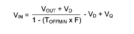
Now if we use this for a 12V output:

VOUT: 12V, Iout: 300 mA
VD: Diode:  0.5V
TOFFMIN: 300ns
Fmax: 600kHz (max. Value according to the datasheet)
VQ: internal Mosfet deop 0.5V

We get a VIN_Min of 15.2V


If we use the current datasheet (2014 Rev), the formula is different:

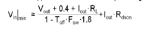
Now in this case, for the same VOut of 12V, 300mA

VOUT: 12V, Iout: 300 mA
Rdson:0.32 Ohm (max. Value according to datasheet)
TOFF: 300ns

Fsw_max: 600kHz
RL: 0,41Ohm k

We get a VIN_Min of 18.6V, which is significantly different from the result we got from the first formula.

Complicating this further, when I try to simulate in WEBENCH the two configurations with the different VIN_Mins, I get the following message (for the 18.6V VIN_Min):

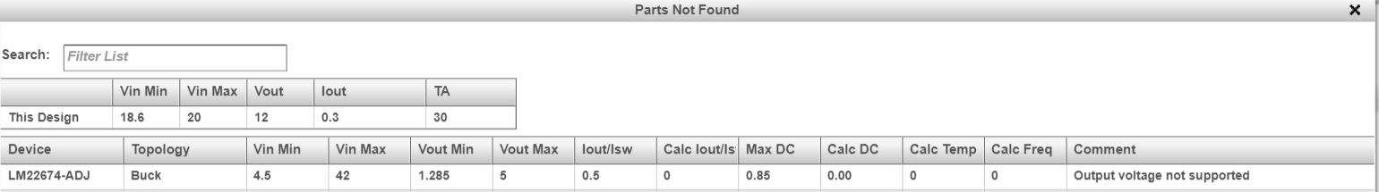
It seems that WEBENCH thinks that 18.6V is too low for the 12V 300mA output.

Also the lm2267x-22680design-calc 


Thanks and Regards,

Mihir Gupta

FAE - South Germany

  • Sorry, it seems like half of my post was cut off. Continuing the post:

    Also the lm2267x-22680design-calc tool seems to be unavailable for download:

    The questions are:
    1. What is the correct formula for VIN_Min?
    2. Is WEBENCH showing the correct results?
    3. Could you provide me with a copy of the LM2267x Design Calc tool?

    Regards
    Mihir Gupta
  • Hi Mihir,

    I also got an error when i simulated the design from the product folder . But once i was at Webench home screen and entered the specification , i could search the solution based on LM22674 . I will communicate the same with Webench team and will ask them to fix it .

    As far as the dropout specification is concerned , The Min voltage is calulated as :

    Drop due to Max duty cycle limit(min off time)+ drop across high side FET + drop across the inductor .

    The see a factor of 1.8 on denominator which was not there earlier . I need to see why was this added later . Will get back to you on this soon .

    ---Ambreesh
  • The 1.8 factor takes into account the worst case values in the data sheet.

    You use the typ values in the equation and the 1.8 takes care of worst case.

    The equation in the latest data sheet is correct; worst case.