This thread has been locked.

If you have a related question, please click the "Ask a related question" button in the top right corner. The newly created question will be automatically linked to this question.

UCC27211: UCC27211 Issue with Short Pulse Widths

Part Number: UCC27211
Other Parts Discussed in Thread: UCC27282, UCC27800

I have a customer who has seen the following when decreasing the duty-cycle of the HI/LO pulse widths to <50ns. The reason I mentioned 50ns is that the data sheet states that the minimum pulse width that is need to change the outputs is 50ns. I have explained this to the customer and he understands the data sheet specifications, but is wondering why the device reacts in the manner that it does. He stated the following:

The datasheet says, and this is quoted from the datasheet, “Minimum input pulse that changes the output - 50ns max”.  To me that says that if you provide pulses narrower than 50ns there is no guarantee that the output will change state in response to the narrow input pulse. It doesn’t mean that the output behavior is completely undefined if it is provided with narrow pulses. 

He believes that the device should not respond to these short pulses at all. I explained that this was not the case, but he still wants an explanation of the behavior that he is seeing. I understand if you do not directly address his questions, but I am submitting them because he has requested that I do. His response was this:

How an IC responds in corner case conditions that are likely to happen (even if the spec sheet is written to steer users away from it) is what separates a cheap knockoff and a premium brand. I would appreciate it if you could provide my feedback to your R&D team for consideration in your future designs. As an R&D designer I would appreciate to hear detail application related issues regarding my design.

I have included 4 scope shots of the response of the UCC27211. They are as follows:

UCC27211-1 shows conditions where both HI and LI have sufficient pulse width to actuate the FETs

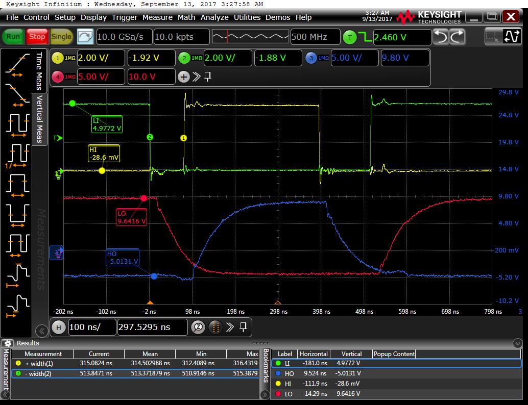
UCC27211-2 shows narrower duty cycle where the HI is no longer being actuated and LI is the only one being actuated and still controlling the SyncFET.

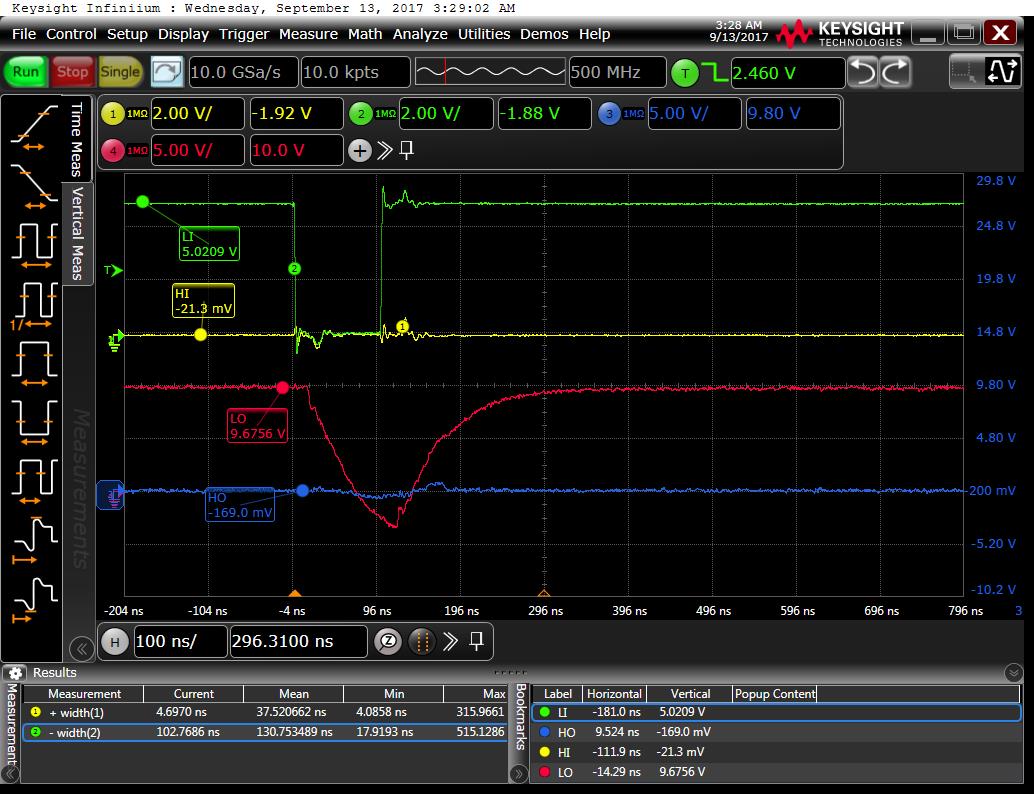
UCC27211-3 shows yet narrower duty cycle right before the IC shows the pulse width distortion. The SyncFET is still slightly modulated.

UCC27211-4 shows even narrower duty cycle where now the LO pulse width is roughly 280nS wider than LI.

So a very narrow pulse width actually produces a “long” pulse on the output. Can you explain what is happening here?

Thanks for your help with this!

Richard Elmquist

  • Hi Richard,

    Thanks for your question, and Thanks for the R&D feedback!

    This is a known issue with this part -> a narrower input pulse producing a wider output pulse.
    This is due to the design of the input stage, when the input pulse widths are very narrow then the drive for the output stage is smaller leading to the output stage of the driver to also be less. This is why the time it takes to respond to an input is longer. Basically, when the input pulse widths are small, current coming out of the input stage is less therefore the drive coming out of the output stage is less. Becuase of this the delay becomes longer and manifests itself as a wider pulse width.

    Does this make sense? I will work on a more precise answer for why this issue occurs and update you asap.

    Thanks,
  • Jeff,

    Please send me your final answer as soon as you can so I can provide this to the customer.

    One question: Is that why the minimum pulse width needed to change the output is listed at 50nS? The reason I ask is this seems to be where the customer is not understanding the issue. He has seen that if he does not exceed this issue that there are no problem. I just wanted to make sure that I am reading the data sheet correctly.

    Thanks for your help with this!

    Richard Elmquist

  • Hi Richard,

    No problem, Im glad to help!

    UCC27211 employs an asymmetrical level shifter which has a fast and slow path. The level shifter is not edge triggered rather is On-Off-Key triggered and when HI is in high state, the level shifter output is actively being set high. A one-shot-path is added to match rising and falling delay however the one-shot-path does not have enough pullup when input pulse width is narrow. This results in the propagation delay being longer with the narrow input pulse, thus the output pulse width is wider.

    This occurs for both LO and HO when a narrow input pulse occurs. It also occurs for tempertaure and HS voltage exceeding upper limitations, and VDD or HB-HS exceeding lower limitations. The value of 50ns comes from extensive testing and simulation: with <50ns pulses at 12V VDD HO and LO are 105ns and 60ns respectivly. It is also tested at 8V VDD and LO remains at 60ns and HO increases to 175ms.

    Output pulse width stretching on legacy drivers can be avoided by incorporating a minimum pulse width clamp in digital controllers or placing RC filter at the input for analog controllers.

    Similar corner testing was done on UCC27800 and UCC27282, the results have a lower minimum pulse width specification. When input pulse width is reduced below specification limit, the output pulse does not stretch, that is, when input pulse width is reduced beyond the point it is properly recognized by the input stage of the driver then the output of the driver is held low. As with any other driver, the switching parameters change as VDD and HB voltage changes in either direction.


    I hope this satifys your customer! Please let me know if you have any more questions!
    Thanks,
  • Jeffrey,

    Thanks for your detailed response! I really appreciate this.

    Have a great weekend.

    Richard Elmquist

  • Thanks Richard!

    You toooo! I will close this thread, but feel free to reopen if clarification is needed!

    Thanks,