Because of the Thanksgiving holiday in the U.S., TI E2E™ design support forum responses may be delayed from November 25 through December 2. Thank you for your patience.

This thread has been locked.

If you have a related question, please click the "Ask a related question" button in the top right corner. The newly created question will be automatically linked to this question.

BQ2205LY: BQ2205LY

Part Number: BQ2205LY

Is the /RST output supposedly connected to the Reset input of a microcontroller?

We are handing external battery backed SRAM and experienced memory loss during power cycling. We are not using the /RST output since on datasheet is described as optional.

Can you clarify that?

Thanks,

  • Hi Eduardo

    The RST pin is dual function. It will generate a reset or it can be used to reset the device with an external button press.

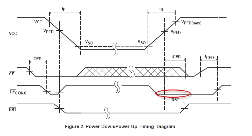
    Figure 2 shows the “generated” reset. Basically, the device backs up an SRAM with a coin cell when the main power supply (VCC) drops below VPFD. It holds it low – potentially preventing the controller from trying to do something as power fails or before it fully recovers. It holds the RST pin low for tRST after VCC recovers.

    CE (SRAM Chip Enable) is the input to the device and CECON is the “conditioned” CE. Figure 2 also shows CECON as VCC fails. Actually CECON1 and CECON2 for 2 SRAM banks if needed. Table 1 shows the Truth Table of CE/, A (address or bank selection pin), CECON1 and CECON2. As noted earlier, if power fails, the CECON pins are high.

    As an input, if the push-button is held low for “tPBL” (Push Button Low) then the bq2202LY will hold the RST pin low for an additional tRST which will generate a reset for the system. Note that a very small push button (1µs) can generate a “long” 30ms to 85ms pulse on RST.

    In no cases will the RST function (internal or external) impact what’s going on in the CECON pins. So, RST will NOT impact the memory.

    When memory is corrupted, it’s usually one of a few issues.
    1. The slew rate on VCC is too fast (see tF). Add more capacitance to VCC.
    2. Pins going below ABS max (-0.3V). This can cause all sorts of issues, but mainly it can cause loss of data. Cause of this can be poor ground, poor isolation or a variety of other issues. Possibly floating RST with a negative spike?

    Quick problem identifiers:
    A. Check VCC slew rate on failing supply.
    B. Check all pins for negative undershoots.
    C. Pull RST high.

    thanks
    Onyx
  • During power up the /CECONX still low during tCER (see circled) and enabling the external SRAM. Shouldn' t be using the /RST output to prevent memory problems?

  • Eduardo,

    The drawing in Figure 2 is incorrect.  The CECON1 and CECON2 pins will remain high until tCER after VCC rises through VPFD.

    Once tCER is met, they will follow CE. This should be able to be verified with an oscilloscope on VCC and CE, CECON1 and CECON2.

    The RST pin does not impact the CE pins at all.

    Regards,

    Dick