This thread has been locked.

If you have a related question, please click the "Ask a related question" button in the top right corner. The newly created question will be automatically linked to this question.

TPS65193: 50Hz +-15V/+-24V PWM Generation Circuit

Part Number: TPS65193
Other Parts Discussed in Thread: TLV61046A, TPS65131, PMP9780

Hi team,

My customer is designing a 50Hz +-15V/+-24V PWM Generation Circuit, we found TPS65193 a good fit for this application, we have some questions about this wish you could help: 

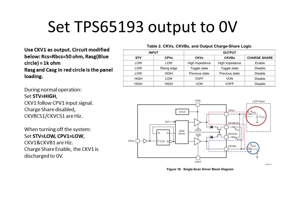
1. For TPS65193, customer need to turn off this circuit when not used, this requires TPS65193 output to be 0V (GND) when turning off. One method is to turn off the power supply; but we are think about to use TPS65193 charge share function to do this.

For example, like the Figure 18 block diagram below, we use CKV as output, and CKVB connect to GND through Rasg (1k ohm) (No Casg cap). During normal operation, set STV=high, CPV as input; during disable, set STV=Low, CPV=Low, Charge Share enable, CKV should be pulled to GND. Is this correct? 

2. We have promoted TPS65131 for +-15V power supply, but for +-24V power supply, we don’t have a good idea to do it right now. We are thinking about using a Boost like TLV61046A output 13V voltage, and using charge pump to generate +-24V, but we are a bit concern about its transient response as there is no feedback. Do you have any suggestion for +-24V power supply?  

3. Although TPS65193 is available on ti.com, we haven’t found its EVM on ti store, would you please suggest if there is a EVM available and how to apply it? Thanks. 

Kevin

  • Hello Kevin,

    1) Does this mean that you will only use the CKVx as output and do not connect CKVBx to the panel? What about the corresponding xCSx-channels? I will need to check in the lab if this is possible, but I see doubts as If CPVx is LOW the outputs will be pulled against VOFF.

    2) What I can suggest is to use the reference design PMP9780 (with regulation of +/-24V) and modify it. You will need a double-inverting stage to get -24 V. Take care on the ratings of the components. Will this be an acceptable solution for your customer?

    3) There is no official released EVM of this device. I can send you an SEB offline.

    Thank you.
    Best Regards.
    Ilona
  • Hi Ilona,

    1. yes, we only need 1 output channel, which is CKV1. CKVB1 is connect to GND through a 1k ohm resistor (like the Rasg in Figure 18 but no Casg). CKVBCS1 and CKVCS1 should also be connected like figure 18 and Rcs/Rbcs could be 0 or 50ohm.

    this circuit would add extra power consumption on Rasg 1k ohm resistor during normal operation, but it should be OK.

    2. thanks for your suggestion, I will double check with customer.

    Kevin

  • Hello Kevin,

    Regarding 1)
    When you say CKVB1 connect to GND through 1k ohm resistor. Are you also planning to connect this node to the pin CKVB1?
    The problem I see here is that as soon as CPV1 is pulled Low the output-pins (CKVx) will be pulled against VOFF (table 2). The load of RASG and CASG (although not connected here) will define the discharge time to be pulled against VOFF.
    What I can think of is to use an external resistor divider (VON(CKV) to VOFF) and tab it to have 0 V. This could define your CKV if CPV1 is LOW.... let me check this in more detail and I (hopefully) can give a draft tomorrow.

    Best Regards.
    Ilona
  •  Hi Ilona,

    I have received the notice for SEB shipment, it should arrived tomorrow. thanks for your support.

    Please check below picture about the turn off circuit and your suggestion is appreciated. 

    Kevin