This thread has been locked.

If you have a related question, please click the "Ask a related question" button in the top right corner. The newly created question will be automatically linked to this question.

TPS56121: Device failure in 12V to 3.3V 15A configuration

Part Number: TPS56121

We are facing a serious device failure when powering a TPS56121 with 12V. The device somehow breaks and forwards the 12V to its output, thus burning all the ICs on its output power rail. The device is configured to output 3.3V up to a maximum of 14A and it is enabled by another TPS56121 that generates 1.1V@15A, which seems to work properly.

We are having difficulties in understanding why this happens because it happens randomly. We have inspected carefully the PCB and it seems that there are no issues in manufacturing.

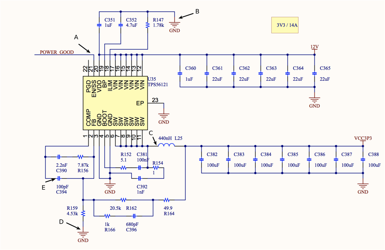
I'm attaching a schematic drawing of the TPS56121, is there anything wrong?

  • Giancarlo,

    It appears you have mostly copied the schematic from the datasheet.  To start, you may want to remove two of the output capacitors so that it matches exactly.

    It is most likely an issue with the EN/SS circuit.  I would not drive it directly with PGD.  Try disconnecting that line and connect 33 nF directly from EN/SS to GND.  If this solves your issue, we can work out a sequencing scheme.

    If the high side FET is shorting out and it is not the EN/SS, the next most likely cause is you are subjecting it to an over voltage condition.  It may be excessive overshoot or ringing on Vin or SW.  On SW also check for excessive negative excursion below ground.  When checking the SW node waveforms use a very short (< 1cm) ground lead as close to the IC pins as possible.  What about your PCB layout? did you follow the guidelines closely?  How far away is your input supply?  You may need to include some bulk capacitance on your input.

    If you can post your waveforms, we can look for anything that might be suspect.

    Let me know if these suggestions help.

  • Hi, Giancarlo,

    From the description, seems the high side FET was damaged and became short circuit.

    I would check the schematic and get back to you soon.

    Meantime, I would suggest contacting local quality team to submit FA request to follow up.

    Thanks.

    Best regards,

    Ray Chen

  • Hi, Giancarlo,

    The loop of both rail are stable.

    For the 3.3V rail, since there is no capacitor attached to EN/SS pin, the soft-start time could be less than several micro-seconds, which would result excessive inrush current flowing through the inductor during start up. In that short period, if the inductor is saturated due to excessive current, the SW node point is equivalently shorted to GND, which can potentially damage the high side FET.

    To proceed on debug, I would suggest verifying 3.3V rail inductor current during startup, checking whether the inductor would be saturated. As suggestion for solution, adding EN/SS cap. is worthy to check.

    Thanks.
    Best regards,
    Ray Chen
  • Thanks for the answers. Just to be sure, are you suggesting to:

    1) cut the path from PGD to EN/SS and to add a 33 nF capacitor from EN/SS to GND

    or

    2) add a 33 nF capacitor from EN/SS to GND and keep the connection between PGD and EN/SS?

    There is one thing that I do not understand though, the chip is supposed to provide over-current protection (for currents above 35A) and our inductor is supposed to saturate above 35A. Is that disabled during startup?

    What waveforms should I post?

  • Hi, Giancarlo,

    For debug, I intend to suggest isolating the rail from PGD first, which will be #1 approach. If #1 can eliminate the risk of damaging the high side FET, then you can move to validate the impact from PGD.

    For the high side over-current protection, current sensing circuitry usually need a blanking time to avoid sampling the switching noise after high side turning on, During start up, the high side OC protection is enabled, but it's possible within limited cycles, the actual PWM pulse width is shorter than the blanking time, then the high side OC circuit is equivalently disabled in these switching cycles.

    Regarding the waveforms, I would suggestion measuring inductor current, switching node, EN/SS and COMP during start-up.

    Thanks.

    Best regards,

    Ray Chen

  • Hi Ray,

    We measured, as you suggested, the waveforms at the switching node, EN/SS and COMP. Please find attached in this post the photos of the waveforms as seen in the oscilloscope, together with the schematic in which the nodes are highlighted where we made the measurements. BOARD A has been modified according to your suggestions, while BOARD B has not.

    Do you see anything meaningful in them?

    Thanks,

    Pietro 

    Schematic


    Ve-Vd (COMP), BOARD A


    Ve-Vd (COMP), BOARD B


    Vc-Vd (SW), BOARD A


    Vc-Vd (SW), BOARD B


    Va-Vb (EN/SS), BOARD A


    Va-Vb (EN/SS), BOARD B

  • Hi, Pietro,

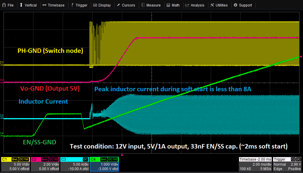
    A start-up waveform is attached below for your reference.

    From the waveform, the output voltage takes ~2ms soft-start time to ramp up; during this interval, the peak inductor current is less than 8A.

    Could you please add a 33nF cap. between  EN/SS pin and GND in your application board and collect similar waveform?

    When there is no EN/SS cap., the soft-start time would decrease to micro-seconds, peak inductor current could be excessive.

    Thanks.

    Ray Chen