This thread has been locked.

If you have a related question, please click the "Ask a related question" button in the top right corner. The newly created question will be automatically linked to this question.

TPS40400: Constant Current Solution issue

Part Number: TPS40400
Other Parts Discussed in Thread: INA139, TLE2144, LM4041C, TPS543B20, TPS543C20, OPA4313, TPS544C20

TI,

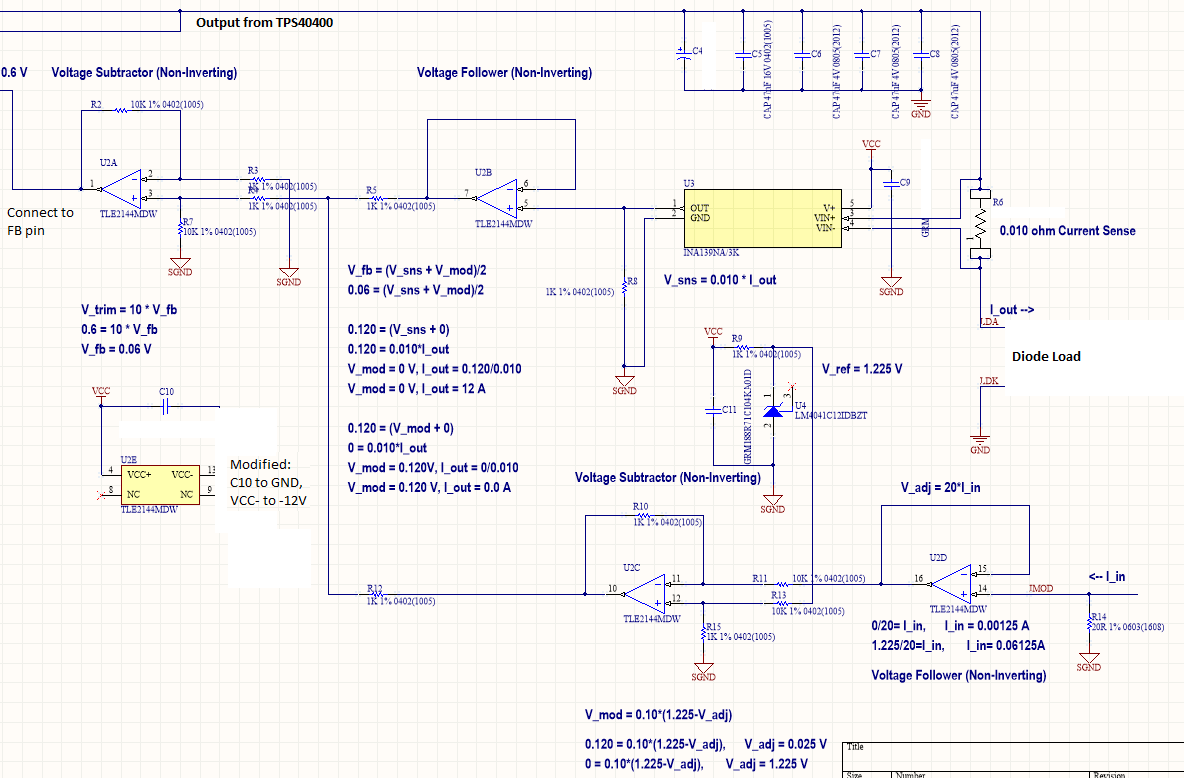
We are working on a solution which employs a TPS40400 based DC/DC, INA139 (Current Sense), TLE2144 (Quad Op-Amp), and LM4041C (Voltage Reference).

The desired behavior is to control the current output of the DC/DC using the FB pin on the TPS40400.

We have produced a bench prototype for evaluating the setup, and have verified the setup is wired as expected. **More details are below.**

When we turn on the setup, the PGOOD is high, and the FB is measured to be 0.612 V. We have an IADJ pin that we feed into the op-amp to adjust the current, and this is set to 0V. The measured output voltage is 0V. All is good. 

When we begin to increase the voltage at the IADJ pin, the FB voltage begins to decrease. Once FB hits about 0.600V or slightly below, the PGOOD goes low, and the FB voltage suddenly jumps to 1.235V and the measured output voltage jumps to 0.750 V. This is unexpected behavior.

**DETAIL ON THE DESIGN**

The INA139 is a High Side Current Shunt Monitor. It is used to measure the current through a 0.010 Ω Current Sense Resistor (Rs).

The current to be measured ranges from 0 to 12A. 

The transfer function of the INA139 is VO = (Is) (Rs) (RL) / (1kΩ) .

For ease of math, we have set the gain (RL) = 1kΩ . This gives VO = (Is) (Rs) = 0.010 * (Is)

(which produces a 0 to 120mV full scale sense input voltage, valid for the INA139)

--

This is passed to a unity gain TLE2144 buffer stage (non-inverting).

The IADJ input is similarly passed to a unity gain TLE2144 buffer stage (non-inverting).

The IADJ voltage is passed into the Inverting (-) input of another TLE2144 stage, and the 1.225V LM4041C reference voltage is passed into the Non-Inverting (+) input. This op amp stage has a gain of 0.1

Thus, VA = 0.1 * (1.225 - IADJ).

Both VA and VO are connected to FB through the last TLE2144 stage to a voltage divider (with equal R values) connected to the Non-Inverting (+) input. The Inverting (-) input is connected to GND. This opamp stage has a gain of 10.

FB = 10 * (Vdiv - 0) = 10 * Vdiv

Vdiv = (VA + VO) / 2

FB = 10 * (VA + VO) / 2 = 5*(VA) + 5*(VO) = 0.5*(1.225 - IADJ) + 0.050 * (Is)

The TLE2144 is powered from +12 V and -12 V rails. (to ensure a full swing to ground)

============================

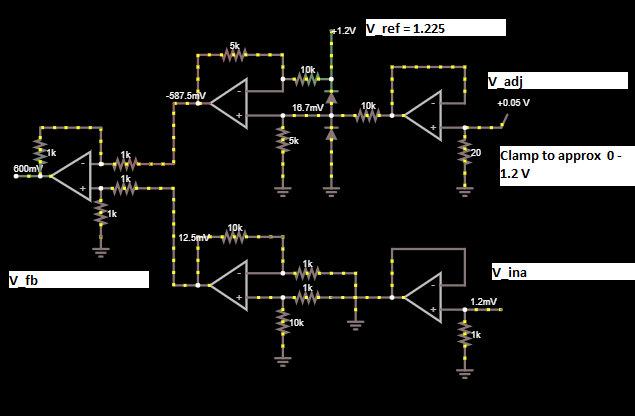
Our transfer function is repeated here for clarity:

FB = 0.5*(1.225 - IADJ) + 0.050 * (Is)

============================

The intended behavior is as follows: 

0.6 = 0.5*(1.225 - IADJ) + 0.050 * (Is)

[[ MAX CURRENT: (12A) ]]

IADJ = 1.225 - ((0.6 - 0.050 *12)) / (0.5)

IADJ = 1.225 V

[[ MIN CURRENT: (0A) ]]

IADJ = 1.225 - ((0.6 - 0.050 * 0)) / (0.5)

IADJ = 0.025 V

================================

Worth noting is what happens if IADJ is 0V.

Is = (0.6 - 0.5*(1.225 - 0)) / 0.050 = -0.25 A

================================

The issue is that the unit will successfully start up with IADJ = 0 V, and will have a current of 0A (because the TPS40400 will not allow the negative voltage, and this is especially true if the load is a diode/LED.) However, as soon as it hits the "turn on" current threshold, IADJ = 0.025 V or so, the unit will immediately "jump" to a FB value of 1.235 V (not 0.600) and the output voltage will sit at 0.750V (may not be relevant if a diode load). 

Given the above detail, we would expect that  (1.235 - 0.5*(1.225 - 0.025)) / 0.050 = 12.7 A which would imply that the output is not being properly regulated. Indeed, the measured output of the INA139 is 0.127 V or 0.010 * 12.7A. 

Why would the TPS40400 FB pin not hold at 0.600V? Any ideas why it might be higher than anticipated? 

The correct behavior for this scenario should be 0A, (0.6 - 0.5*(1.225 - 0.025)) / 0.050 = 0A

It is also worth noting that increasing the IADJ value does not change the FB value, (which is expected, but not at 1.235), and does change the (Is) value.

Any insight or suggestions on what else to check are appreciated.

Thanks,

  • I will test this again with a LM4050 instead of a LM4041.

    Using a 2.5 V reference instead of a 1.225 V should shift the following:

    ============================

    1.235 = 0.5*(2.5 - IADJ) + 0.050 * (Is)

    [[ MAX CURRENT: (12A) ]]

    IADJ = 2.5 - ((1.235 - 0.050 *12)) / (0.5)

    IADJ = 1.23 V

    [[ MIN CURRENT: (0A) ]]

    IADJ = 2.5- ((1.235 - 0.050 * 0)) / (0.5)

    IADJ = 0.03 V

    ================================

    And for completeness:

    if IADJ is 0V.

    Is = (1.235 - 0.5*(2.5 - 0)) / 0.050 = -0.3 A

    ================================
  • BGX,
    It would be very helpful if you could post your schematic.
  • If there are confidentiality issues schematic can also be emailed. Please let us know.

    Mathew

  • See response to John
  • If the circuit is working properly then the FB voltage should not jump to 1.235V. Try to isolate the circuit and see if you can test this scheme in stages or independently. It looks like an open f/b issue loop issue.

    Mathew
  • Following up.

    I went ahead and broke down the circuit into its constituent parts. Namely the omp amp feedback current sense and the dc/dc converter itself.

    I have determined that the DC/DC is fully functional as intended independent of the feedback loop. The measured DC/DC independent of any feedback mechanism is as follows:

    V_in = 11.8 V 
    V_fb = 0.601 V
    V_out = 0.602V

    This is correct behavior with no feedback resistor connected between between the FB pin and Ground to set the output Voltage.

    ============

    Secondly, the Op-Amp Current Sensor feedback also appears to work correctly:

    With no load current, (V_s = 0), the VADJ works properly:

    Assuming Vo is the output to the FB pin normally:

    Vo = 0V when VADJ = 1.225 V
    Vo = 0.613V when VADJ = 0V

    =============

    So the issue appears to lie in how the Op amp stage is connected to the FB pin.

    Right now, there is NO resistor, the output from the op-amp is directly connected to the FB pin. FB is not connected to anything else.

    =============

    However, with some experimenting, adding a resistor divider stage AFTER the op amp and BEFORE fb input has an significant impact.

    I created a divider with three resistors. One 20k, 10k and one 220 ohm, from the (op amp output) <-220--> (FB) <-10k--> (signal ground). 

    The 20k is between DIFFO and FB. 

    This has been largely trial and error, experimenting with solutions.

    This is closer because the output of the TPS40400 at least rises to the point of the diode forward voltage, and FB is measured to still be 0.601V.

    However there seems to still be something going on here that isnt quite right, since :

    (1) I directly connect the op-amp output to the 220 ohm end, seems like nothing is happening.

    (2) I disconnect and then reconnect the output to the 220 ohm end, and it blinks my led briefly (at its lowest setting) and turns off again.

    (3) I increase the current setting before I reconnect, disconnect and then reconnect the output to the 220 ohm end, and it blinks my led briefly again - this time brighter. (I can keep doing this and the LED gets brighter and brighter demonstrating that there is *some* level of control.)

    Closer, but any assistance would be handy.

    Thanks.


  •   

    I wanted to update you on my latest finding. I have determined that the current solution will not work.

    Fundamentally the TPS40400 is a "Voltage-Mode" controller and in order to achieve my desired functionalityI would need a "Current-Mode" Controller.

    Unless there is some method to "convert" a voltage mode controller to a current mode controller, then using the TPS40400 is not an option in this case.

    It seems that TPS543C20 or TPS543B20 would be a better choice in this application, unless you have a better recommedation.

    Regards,

    B

  • BGX,

    Technically there is no reason why you cannot use a voltage mode controller. Even current mode control uses voltage feed back to the input of the error amplifier, the same as voltage mode. What you have to do is convert your current sense signal into a voltage equivalent so that the input to the FB bin is a nominal 600 mV when you have the desired output current. The art in this is stabilizing the entire loop.

    Can you tell us the general design requirements for your application (input voltage range, output current range, what kind of load you are driving)? Do you need PMBus communication? If so, what are you using the PMBus to control?

    We may possibly have a reference design close to what you are trying to achieve.
  •  

    That was my initial thinking when I selected the TPS40400. To address this behavior, I even went as fas as to redesign the feedback circuit to be a bit more concise for what I was looking to do.

    The below circuit is the adjusted version. The TPS40400 has a V_fb of 0.6 V. My R_sense is 0.010. and my maximum current is I_sense = 12A. Again I will walk through my logic here again.

    ---- 
    The transfer funtion of the INA139 is V_ina = I_sense*R_sense*R_L /(1k) . I have selected R_L = (1k) This reduces the transfer function to  V_ina = I_sense*R_sense . This is buffered through a unity TLE2144 stage. This converts the current sense signal to a voltage signal.
    This buffered V_ina is fed into another TLE2144 stage with a gain of 10, making the final transfer function:
    V_out =  10*V_ina = 10*I_sense*R_sense
    ----
    The feedback voltage of the TPS40400 is V_fb = 0.6 V
    My resistor divider uses  499 ohm and 499 ohm resistors. 
    ----
    My TLE2144 setup with the  LM4041C  1.225V reference has the following transfer function at unity gain. (first a buffer, then a unity subtractor). V_adj is the input, V_cntl is the output.
    V_cntl = 1.225 - V_adj
    ----
    Thus the complete transfer function should be as follows:
    V_fb= (V_cntl + V_out) /2 

    V_fb = ( 1.225 - V_adj + 10*I_sense*R_sense) / 2
    0.6 = ( 1.225 - V_adj + 10*0.01*I_sense) / 2
    1.2 =   1.225 - V_adj + 10*0.01*I_sense 
    Thus when V_adj = 0 V
    1.2 =   1.225 + 10*0.01*I_sense
    -0.025 =  10*0.01*I_sense 
    I_sense  =    -0.0025/0.01 =  -0.25 A ( but the INA139 cannot swing negative so 0A )
    I_sense  = 0 A
    Thus when V_adj = 1.225 V
    1.2 =   10*0.01*I_sense
    1.2 =  10*0.01*I_sense
    I_sense  =   12 A
    When my circuit powers up with V_adj = 0, I get ~0.613 at the FB pin. Which is fine and expected.

    As I increase the voltage at V_adj the voltage V_fb begins to drop. This continues until approximately until V_fb = 0.600 V at which point the TPS40400 appears to "turn on". This occurs at Vadj ~ 0.025V. Which is also fine and expected.
    HOWEVER, the voltage at V_fb becomes wildly unstable.  It can jump as low as 0.5 V and as high as 1.2 V and never seems to stabilize. 
    I am driving an LED load with a V_f of 1.2V and I_th of 0.7 A.

  • To add why 0.613 is valid:

    V_fb = (1.225 - V_adj + 10*0.01*I_sense) / 2

    I_sense = 0 A
    V_adj = 0 V

    V_fb = (1.225) / 2 = 0.6125 ~ 0.613 (regulator will try to drive ouput low.)

    ---------------
    Then suppose V_adj = 0.010

    I_sense = 0 A
    V_adj = 0.010 V

    V_fb = (1.225 - 0.010) / 2
    V_fb = (1.215) / 2 = 0.6075 ~ 0.608 (regulator will try to drive ouput low.)

    ---------------
    Then suppose V_adj = 0.020

    I_sense = 0 A
    V_adj = 0.020 V

    V_fb = (1.225 - 0.020) / 2
    V_fb = (1.205) / 2 = 0.6025 ~ 0.603 (regulator will try to drive ouput low.)

    -------------
    Then suppose V_adj = 0.030 <======= now above threshold of 0.025

    V_adj = 0.030 V
    V_fb = 0.600 V (regulator will try to drive ouput higher and should succeed)

    I_sense = (1.2 - 1.225 + V_adj)/(10*0.01)
    I_sense = (1.2 - 1.225 + 0.030)/(10*0.01)
    I_sense = 0.050 A
  •   

    I was thinking the instability may have something to do with how the COMP, DIFFO, and FB are connected.

    Taken directly from the datasheet for the TPS40400 I have REMOVED the following connections in RED

    My circuit still has a compensation network connected between FB and COMP, FB and DIFFO. C1, C2, R2 for the COMP network and C3 and R3 form the DIFFO network.

    I removed the 20k resistor I had for R1. R_bias is also no longer connected.

    Rs1 and Rs2 are both 10 ohms, but I have disconnected both of these from the output entirely (Vout and GND).

    My feedback circuit is connected to FB directly.


  •   

    I have another update. 

    I have fixed the instability issue by removing some of my output capacitace. 

    Currently I have 3 x 47uF , 1 x 0.047uF as the output capacitance on the TPS40400 and that seems much happier.

    =========

    It seems we are very close now to this functioning correctly.

    The only issue now seems to be the issue I described before, where the V_fb continues to drop as V_Adj increases because there is no output current.


    For example, at V_adj = 0.125 V, which is well above the 0.025 V at which the unit reaches V_fb = 0.600 V and turns on.

    The expected behavior is:

    V_adj = 0.125 V

    I_sense = (1.2 - 1.225 + V_adj)/(10*0.01)

    I_sense = (1.2 - 1.225 + 0.125)/(10*0.01)

    I_sense = 1 A

    However, because I_sense never increases, I am getting:

    I_sense = 0 A

    V_fb = (1.225 - V_adj + 10*0.01*I_sense) / 2

    V_fb = (1.225 - 0.125 + 10*0.01*0) / 2

    V_fb = (1.225 - 0.125) / 2

    V_fb = 0.550 V     <========== this is the measured value I am receiving for V_fb

    This trend continues regardless of what the value for V_adj is.

  • I ran a basic sim on your circuit. The simulation operates mostly the way you describe with your FB point quickly railing out around 1.21 V. Looks like you will need to re-think your control scheme.
  • Brian,
    What are your plans going forward? If you can share some details about your application, we can help you with your control scheme. Let us know.
  •  

    I want to appreciate why this control scheme would not work (as well as my initial control scheme design) before I move forward with designing yet another control scheme.

    In the end, the design requirements are the same --- Constant Current Control of the TPS40400 . The load would normally be an LED.

    ====

    The input source should always be able to reasonably operate with an input 5 to 14V. It may be desirable to operate the regulator with a lower input voltage as close as possible to the operating voltage of the LED  point of load to decrease the power dissipated by the regulator at high currents. The TPS40400 has a fantastic 3-20V wide input range, that makes it perfect for this purpose. PMBus is a nice feature to have to access the regulator data and store information on the load that it is driving.

    The current output should have a method of controlling/selecting the output current dynamically with a voltage input signal (i.e. from a DAC).  This modulation should be capable of at least 1kHz, higher modulation rates are more advantageous. The TLE2144 selection has substantial bandwidth to deliver a control signal to the TPS40400. Ultimately it is the regulator circuit that will limit the maximum modulation speed.

    We chose the TLE2144 because it can be driven directly by the input voltage of the TPS40400 without issue, and using a voltage inverter, we can drive the negative rail without issue as well.this works over the entire range of the TPS40400. (i.e. +20 input would give +/-20 for the TLE2144, giving a 40V rail to rail or +3V would give +/-3V or 6V rail to rail. We considered using the OPA4313 instead, but we needed a separate regulator to provide the +/-5V for the unit.

    The output is only designed to drive one single high-power LED/array. The output should have a maximum output of at least 5.5V, which is sufficient to bias most individual diodes. The output voltage is obviously limited by the input voltage. It may be necessary to drive the load up to at least 12A.

    The INA139 provides a convenient feature to adjust the gain of the entire system. by increasing R_L, (eventually using a 100k POT) we hoped increase the gain of the output from unity to 101. This ultimately would allow us to set the maximum current limit of the entire system. In our previous designs, a 10x gain would drop the maximum output current from 12A to 1.2A , and 100x gain would drop it to 0.120 A. The control (V_adj = 0 to 1.2V) would stay the same. This is highly desirable.

    The effective current range of the output current through the diode would be 0.120A to 12A max.

    ===

    I'm trying to determine what change I need to make to this circuit to at least achieve a most basic level of current control.

    Thanks,

    B

  • It is pretty easy to set up TPS40400 as a constant current source.  The tricky part comes in if you want to have a variable current source.  I simulated your original circuit and teh FB node did rail out to 1.2XX V as you observed.  The needed result is to have the VFB voltage be 0.6 V when the current is at the level set by your control.  What are you planning to use as your variable current control? Will you use an externally supplied voltage or a variable resistor or other?

  •  

    I believed this to be a fairly straightforward solution too, since I have implemented this similarly with other DC/DC converters.

    The reason it is railing out at 1.2V is because the current is not increasing.

    In principle, if my final output of the adjustment side of my resistor divider is 1.2V and the output of the current side of the divider is 0V then the divider should produce the required 0.6V at the FB pin.

    I was fairly certain this was how it was "supposed" to work. But there is NEVER any current output. so it rails at 1.2 and then decreases to 0.

    Vadj FB Vsns
    0 0.6 1.2
    0.1 0.6 1.1
    0.2 0.6 1
    0.3 0.6 0.9
    0.4 0.6 0.8
    0.5 0.6 0.7
    0.6 0.6 0.6
    0.7 0.6 0.5
    0.8 0.6 0.4
    0.9 0.6 0.3
    1 0.6 0.2
    1.1 0.6 0.1
    1.2 0.6 0

    This is what is happening:

    Vadj FB Vsns
    0 0.000 0
    0.1 0.050 0
    0.2 0.100 0
    0.3 0.150 0
    0.4 0.200 0
    0.5 0.250 0
    0.6 0.300 0
    0.7 0.350 0
    0.8 0.400 0
    0.9 0.450 0
    1 0.500 0
    1.1 0.550 0
    1.2 0.600 0

  •  ,

    I've taken the weekend to revise my control strategy. I think the following circuit below will behave the way I am hoping, and is centered around the V_fb = 0.6 reference voltage. If you can verify that such a solution might work via simulation with the TPS40400, I would be grateful. I am still strongly considering switching over to a TPS544C20 and it looks like this control solution would work as well.

    I also found this reference handy as an constant current implementation achieved with an INA139 and a TPS buck controller. [For future readers] Just don't get distracted by the TWO separate control loop in this doc... there's one for voltage and one for current. www.ti.com/.../tidrob3.pdf

  • I'll take a look at it tomorrow.
  • Thanks.

    I am looking forward to your response.

    -----

    A few more thoughts.

    I believe this should meet the need, since when the TPS40400 first starts up, no current is flowing out of the output and the proposed control solution natively outputs the ~0.6 V. In reality it will be about 1.225/2 = 0.613 V. This is higher than 0.6 , and therefore the TPS40400 should drive the output low, which is fine in this case.

    As we adjust the Vadj input higher; up to Vadj = 0.025 V,  (1.225-0.025)/2 = 0.600 V the unit should threshold, and "turn on". When Vadj > 0.025 V, the TPS40400  and begin raising its output voltage in an attempt to re balance the FB back to 0.600, because the output setting is now below the 0.600 target.

    For example, if we set Vadj = 0.125V the output of the control stage will be (1.225-0.125)/2 = 0.550 V . Since this is below the required 0.6, the TPS40400 should raise its output to reach the needed 0.600.  In this case, the current output will be:

    0.600-0.550 = 0.050

    0.050/10 = 0.005

    0.005/0.010 = 0.500 A

    The control Vadj input is clamped by two schottky diodes (i.e BAS40-04) to ensure we stay in a healthy range.

    The only catch here is that in the case where I have the full output, say 1.2V, 0.600/(10*0.010) = 6 A . This is exactly half of my desired output range. (12A)

    However, simply reducing the current sense resistor should resolve the issue, and give me a few more range options, pending proper hardware.

    0.010 ohm = 6A max

    0.005ohm = 12A max

    0.003ohm = 20A max

    0.002ohm = 30A max

    By adding a 100k potentiometer in series with the 1k to vary to the RL value from 1k up to 101k, we should still fall within the limits of the INA139 and also be able to adjust the maximum current limit in hardware, in addition to software.

    For example,

    If the desired setpoint is say ~16.7 A. We could select the 0.003 ohm current sense, and then adjust RL

    0.600/(10*0.003*16.7) = 1.19760479k . Or adjust the 100k Pot value to 197 ohms.

    If the desired setpoint is say ~0.100 A. We could select the 0.010 ohm current sense, and then adjust RL

    0.600/(10*0.010*0.1) = 60k . Or adjust the 100k Pot value to 59 kohms.

    For each current sense range we can calculate the minimum current limit value when RL = 101k

    6A max limit  ==> 0.600/(10*0.010*101) = 0.06 A minimum limit

    12A max limit  ==> 0.600/(10*0.005*101) = 0.120 A minimum limit

    20A max limit  ==> 0.600/(10*0.003*101) = 0.200 A minimum limit

    30A max limit  ==> 0.600/(10*0.002*101) = 0.300 A minimum limit

  • I believe you have been over thinking this. A simple seesaw circuit shoud allow you to adjust the output current. I'll post a simplified schematic tomorrow.
  • Brian,

    Try this simple circuit.  With V ADJ = 0 V, you will get maximum output.  Adjust V ADJ up to decrease the current.  You may need to modify the resistor values to suit your specific conditions, but I'm sure you can understand the simple principle.

    Let me know if this works for you.

  • ,

    Certainly understood. This is more or less how I originally started my design.

    Something still seems off though here.....

    In this case, the INA139 will have an output of Vout_1 = I_out*R_s*R_L / (1k) per the datasheet.

    You have selected R_s = 0.010 and R_L = 10k

    Vout_1 = I_out*0.010*(10k) / (1k)

    Vout_1 = I_out * (0.1)

    I see you have adjusted the scaling by using the resistor divider:

    1.1k and 429 ohms

    in the case where Vadj = 0 the current will be at it's maximum value.

    thus with this divider, 

    V_ref = V_iop1 * 429 / (429 + 1100)

    V_ref = 0.6 per the datasheet

    0.6 = V_iop1 * 429 / (429 + 1100)

    V_iop1 = 0.6 * (429 + 1100) / 429 

    V_iop1 = 2.138

    Since you have a unity gain buffer, V_iop1 = Vout_1 = I_out * (0.1)

    2.138 = I_out * (0.1)

    I_out = 2.138 / (0.1)

    I_out = 21.38 A


    There are 3 changes to this design that are in my version of the circuit. 

    (1) on the Vadj side, I have inverted the input so that increasing the voltage increases the current and decreasing the voltage decreases the current, but the output itself is still equivalent.

    (2) I have used a V_iop with a gain of 10 and an R_L of 1k , and this still should be equivalent, since the transfer function is equivalent.

    (3) My resistor divider is equal. With my 499 ohm original example...... and this exact circuit,

    V_iop1 = 0.6 * (499 + 499) / 499 = 1.2

    V_iop1 = Vout_1 = I_out * (0.1)

    1.2 = I_out * (0.1)

    I_out = 1.2 / (0.1)

    I_out = 12 A

    Is there a TI-TINA model for the TPS40400? As far as I can tell it is not available. It would assist greatly.

  • Sorry,

    Looks like only pspice is available. I did not intend for you to use the actual values for resistors. I just put something together quickly to get a screen capture rather than a hand drawn schematic.
  • Brian,

    I would like to close this thread unless you think you need something else. Let me know
  • ,

    Thank you for the quick reply and your time assisting me with this.

    Overall I wanted to confirm my understanding of your most recent seesaw circuit was correct. Since this has more or less brought me back in a big circle if that understanding is correct. Which has become frustrating.

    I'd like one more thing before we close this thread,

    If you take your same seesaw circuit and feed the output from IOP1 into IOP2, an op-amp with a gain of 10 and decrease your R_L from 10k to 1k. Do you still achieve the same result? Can you post that circuit?
  • Brian,

    I'm not sure what you mean. Contact me directly at j(dash)tucker(at)ti(dot)com. We can maybe set up a call and webex tomorrow.
  • ,

    I'm just checking to see if you received an email from me.

    --

    Again, all I did from the previous see-saw you provided was change the 10k R_L for the INA139 to 1k . This changes the gain of the INA139 from 10 to 1.

    And then after the unity buffer I added another op-amp (IOP2) thats setup for a gain of 10 with the output of IOP1 as the non-inverting input.

    The point is that this should be equivalent to the original circuit.

    Im wondering if you get the same result in Simulation if you add this second op amp and drop R_L to 1k.

  • I did not see any email in my mailbox j(dash)tucker(at)ti(dot)com
  • @JohnTucker

    I just sent another email. Please check you Spam or Clutter folders.

    The subject is "Test"