This thread has been locked.

If you have a related question, please click the "Ask a related question" button in the top right corner. The newly created question will be automatically linked to this question.

LM5576: Buck converter failing to provide output voltage (unless at high temperature)

Part Number: LM5576


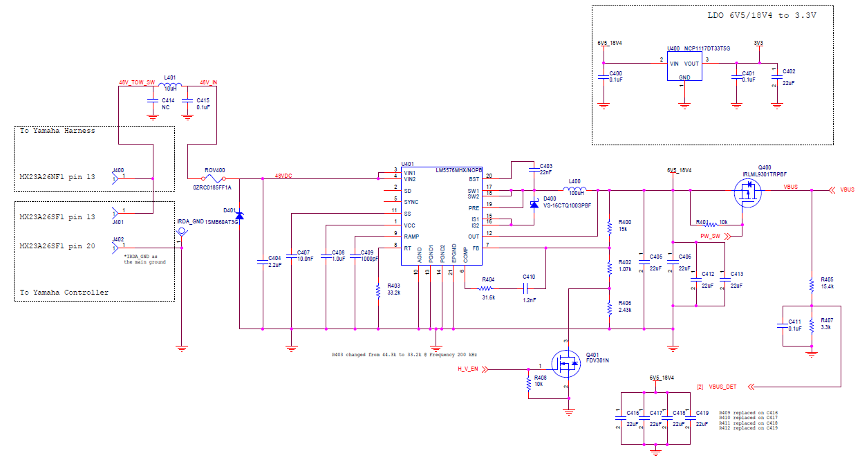
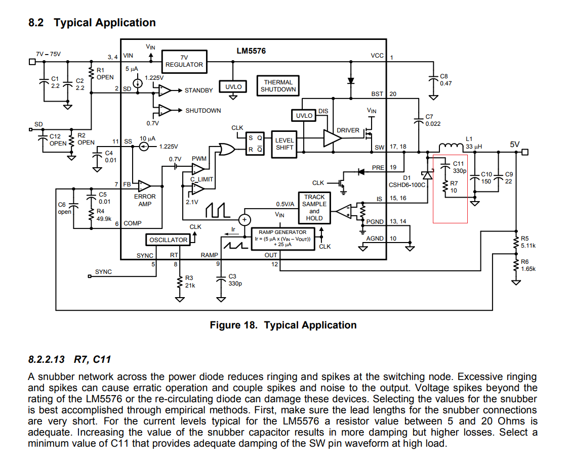
My company has a production PCB which uses the LM5576 to step down power from 48V car battery to 6.5V/18V (option controlled by an on-board MCU using FET Q401). The IC works fine when there is no load connected. However when there is a 4Ω load  (we use this simulate the current draw of our touch-screen tablet) connected at 6.5V output, the IC will fail to provide output voltage or instead give some bad intermediate voltage. Furthermore, the 6.5V also powers a 3V3 LDO which gives power to the on-board MCU, and sometimes this will be reset by our reset monitor, because the voltage dips too much.

Some anomalies to complicate the situation:

1. Our previous board version and current board version only have two changes (ADC accuracy change on the on-board MCU, and higher rating fuse ROV400). We have confirmed neither of these affect converter operation -- however our previous board version works PERFECTLY fine, and always provides output voltage at 6.5V even with 4Ω or ~1.6A current draw; but our current board version is the one that does not output well.

2. The converter works fine when the recirculating diode D400 is heated to 115F, but at room temperature it cannot bring up the voltage.

I am attaching a schematic of the power management section of our design. If anyone has seen this before, or something similar any help would be appreciated in debugging this hardware issue. We are completely baffled over here and at the factory, because there is no sensible reason why this design worked before and not now. If you need any additional details or scope captures, etc., please let me know.

Thanks in advance,

Steven

  • Hi Steven,
    There are multiple issues that could cause the output voltage to fall. A few possibilities are stability, poor layout, and wrong components installed.

    Since you have a working board, I would start by isolating the differences between the two boards.

    Were there any layout changes between the two boards?

    Also, when you say: “Our previous board version and current board version only have two changes (ADC accuracy change on the on-board MCU, and higher rating fuse ROV400). We have confirmed neither of these affect converter,” how have you confirmed this?

    • Have you removed ROV400 on the second board, and powered the device directly at Vin (48VDC)? Have you replaced the ROV400 with the original component?
    • Have you removed Q400 and verified the 4Ohm loaded output without the ADC connected?

    Best Regards,
    Katelyn Wiggenhorn
  • Hi Katelyn,

    Sorry let me clarify, the ADC is on a completely separate block of the board. It in no way interacts with the design here or measures anything on this circuit. The change is simply a resistor and capacitor value change.

    There were no layout changes whatsoever, same copper traces, same board laminate
    •ROV400 went from .85A trip current to 1.85A
    •With second board, ROV400 was removed and jumped, still has bad output
    •The issue persists even if the load is connected without the switch Q400

    While in retrospect I do question the layout myself, I do not think it is the main issue since we have a working previous version with identical layout. Also, I do not believe wrong components are installed as we have manufactured thousands of these boards, and this latest batch of 50 PCBs I have verified components on some myself.

    I am interested in what you mean by stability. Could you elaborate? Often you will hear a high-pitch audible noise (possibly coming from the inductor L400) at each output voltage step (say 0V -> 2V -> 3V -> 4V -> 5V -> 6.5V). Obviously this behavior is non-ideal and the voltage should immediately go from 0 -> 6.5V, as it did with our previous board.

    Also what do you think about the thermal characteristics of the problem? Why might it not work when cold, but then work if heated enough?
  • Hi Steven,

    Would you be able to share a waveform of Vin, SW, VCC, and Vout during both loaded and unloaded during start up and steady state?  Also, would you be able to share the board layout?

    If the loop response of LM5577 is not stable, then there is a possibility for noise injected into the control loop to cause perturbations on Vout or create an issue with output regulation.  The stability will be effected by your L, Cout filter as well as the slope compensation components.  It is possible that by heating up the diode, you are changing the values of certain components causing the design to be stable at this point.

    Best Regards,

    Katelyn Wiggenhorn

  • Katelyn,

    The board layout is below, dimensions are 86 mm x 42 mm.

    I will work on getting you the requested captures.

    Thanks,

    Steven

    Edit: I have removed the board layout images and instead provided a zip (for privacy reasons), because you have already looked at it.

    layout_TB.zip

  • I forgot to mention, when the board is powered by 48V Vin, the converter will work fine and provide sufficient output in this version and previous version. Our problem is that when Vin is 20V, the output is not well regulated to 6.5V for this version -- even though the older version works fine at 20V. We have this use case because the input power supply is a battery.
  • Hi Steven,

    I will look forward to your waveforms.

    Looking at your layout, I do not expect the layout to be the primary problem.

    One test that you can try is adding a bulk capacitor to the input to minimize any ringing at the converter input. If there is ringing at the input, this could cause erratic behavior.

    Best Regards,
    Katelyn Wiggenhorn
  • Hi Katelyn,

    That is good news about the board layout at least.

    Below is a zip of the captures. The file names go as <pin>_<load?>_<time>_<systeminput>. <pin> will be Vcc, Vin, Vout, or SW. <load?> will be load or noload. <time> will be boot or ss (steady state - which I took to be ~30s after boot). <systeminput> is the system input voltage 20V or 48V (scope voltage div is 5V for former, and 10V for latter). So there are 32 captures in total for all possible combinations.

    Let me know if there is anything else you would like me to capture, or experiment on as far as component swapping or the like.

    Thanks,

    Steven

    captures.zip

    Some additional notes:

    • The system input at J400/J401 is a regulated power supply (CS15003XE) at 20V/48V DC

    • I removed mosfet Q400 to ignore any effects of the MCU. I connected load directly from Vout to GND

    • Vout is still suppyling a 3.3V LDO

    • Because of the nature of the problem, I had to turn off power, discharge caps, and cool the board down to room temperature between captures

    • Ignore what I said about 48V working fine. I have not studied the system much at Vout directly, without the mosfet. In any case we can learn more by looking at 48V captures as well

    • I did not get captures of this, but I tried changing input capacitors according to http://www.ti.com/lit/an/slta055/slta055.pdf

    • I tried replacing Vin input capacitor C404 (currently 2.2uF) with 10uF and 100uF caps, no luck for stability. Also tried adding a 10uF cap at C414 (system input), while keeping C404 at 2.2uF, still no luck

  • Hi Katelyn,

    By reading over the datasheet of the IC again, I realized our design left out the optional RC snubber network connected from SW to GND. Looking at the scope images, the inputs/outputs are very noisy when coupled to a high load. By adding the network (180pF cap in series with 10Ω resistor), the board works perfectly fine now!

    Please let me know if you can help confirm this design change to push it forward to my team.

    Thanks,

    Steven

  • Hi Katelyn,

    Hope you had a good weekend. My company's EE still has two questions about this issue:

    • "It seems that you found the solution, great job! Unfortunately, it does not explain why in [previous board version] this issue is not present." -- is there any logical explanation for this? Component values or characteristics just out of spec, where the old board version is stable? Or variation in the lm5576 between production runs, etc?

    • "Today I also tried to add snubber modification with such components Csn=100pF, Rsn=12Ω, the reset issue has gone. Also, I saw that the output voltage shifted from 6.45V to 6.65..6.72V until the board heats up. Have you seen such effects?" -- are there any additional mods we can try, or changing R/C, etc. to reduce this additional instability?

    Hopefully you can guide is in the right direction for making this mod once, so we only see one more final board revision.

    Thanks,
    Steven

  • Hi Steven,

    Thank you for sharing the waveforms and the results of your continued work to debug this issue.

    As you pointed out, the snubber will slow down the switch node and effectively minimize the switch node ringing and noise. Since the snubber fixes your issue, this points to the root cause being high frequency ringing coupling into the control loop from the switch node. To verify if this is different between the two boards, I would recommend taking a waveform of the switch node on the new board and the original board in order to compare the switch node ringing. To compare the switch node ringing of the two boards, it is important to use the 'tip and barrel' method with the scope. This article describes the 'tip and barrel' method. www.eetimes.com/document.asp


    Also, when you say: "the output voltage shifted from 6.45V to 6.65..6.72V until the board heats up" are you referring to the DC value of the output voltage is shifting from 6.45 to 6.65 to 6.72 or that the output voltage is oscillating between these values?

    In order to prevent high frequency noise coupling, I would recommend adding a high frequency bypass cap (100nF) between VIN and PGND. Place this capacitor as close to the device as possible. Another method would be to add a boot resistor in series with the boot capacitor in order to slow down the switch node.

    Best Regards,
    Katelyn Wiggenhorn
  • Hi Katelyn,

    Unfortunately, it looks like my company will not be moving forward with the snubber network or series boost resistor. This would require layout changes, and we cannot do that as we already fabricated a bunch of bare PCBs with the current layout.

    I will continue looking into why the current version fails and previous one works; hopefully that will give us a simple fix such as a component value change.

    Thanks,
    Steven
  • Hi Steven,

    I understand. Let's see if there is a component change which could also help with this issue.

    Were you able to take waveforms of the switch node ringing on both the original board and the new board?

    Best Regards,
    Katelyn
  • Hi Katelyn,

    Please see attached switch node ringing (50ns div) as well as general switching waveform (5us div) for previous board version (v2.0), and new (v2.1).

    Examining the ringing/50ns div, it looks like both boards have identical ringing when the switch is turned on (with 20V Vin, ~10 to 30V ringing at roughly same frequency). However, examining the general waveform/5us div, it looks like the new board is making bad duty cycle and waveform shape, while old board has nice duty cycle and shape.

    Also, our EE and I have both noticed some weird behavior while measuring with oscilloscope probe, where by touching probe tip to SW pin (~15pF, 10MΩ from SW to GND), the output starts to work well.

    With these waveforms, and that in mind, are there any immediate suggestions for improving stability?

    Thanks,

    Steven

    2.0v2.1 captures.zip

  • Hi Steven,

    The scope probe's high frequency capacitance is providing a path for the high frequency noise that is minimizing the effects of the switch node ringing. I believe the noise is coupling to the COMP node and creating instability. Would it be possible to add a high frequency cap (10nF-100nF) between COMP and FB?

    I also used Webench to simulate your LM5576 design. Webench recommends Rcomp=14.7kOhm and Ccomp=3.9nF. You can also try to replace these two components to see if stability is improved.

    Best Regards,
    Katelyn
  • Hi Steven,

    Attached is the Webench simulation.

    Best Regards,

    Katelyn

  • Hi Katelyn,

    Thanks for the update. We will try the modifications to see if it improves stability. I will update waveforms / observations tomorrow.

    In the meantime, this still doesn't address the question of why COMP/SW is stable in the old board version, but not the new one. Because our components for Ccomp/Rcomp did not change at all. Do you have any ideas for why that would be? Could it be a component value tolerance issue? Or tolerance within the specs of the lm5576 itself?

    Thanks,

    Steven

  • Hi Katelyn,

    Our EE and I both tried these mods, as well as playing around with other COMP values. Unfortunately negative effect on the stability of the output. Also measured the ringing/noise on the SW pin, and the amplitude seemed to increase with any mod of COMP components. Please advise on this modification.

    On a side note - are there any other snubber-like mods (which instantly damps ringing, and allows for stable output), which we would be able to drop in on our current footprint?

    Also if you look at the ringing of the switch node in "2.0v2.1 captures.zip", the previous and current board versions have identical ringing. So why is it a problem in one version and not the other? Is there perhaps a secondary culprit for the instability?

    Thanks,
    Steven
  • Hi Steven,

    I believe the LM5576 design is susceptible to the high frequency noise.  This is evident in the fact the snubber fixes the problem, and the scope probe's capacitance also dampens the noise. If noise is injected into the control loop through IS or COMP, I would expect to see erratic behavior.  In order to reduce the switch node noise , you either need to dampen the switch node (snubber - best method because you decrease the amplitude ringing), slow down the switch node (add the Rboot - also will decrease the amplitude but not typically not as drastically), add a high frequency bypass capacitor at VIN directly next to IC (You can try to use a bypass capacitor),  and minimize the output path (Requires Layout Change - Cout GND --> PGND --> IS --> Anode of Diode --> Inductor --> Load). 

    I do not yet understand why the old board did not see this problem and the new board does if the boards are identical besides the two previously discussed schematic change.  How are you measuring the switch node in your waveforms?  Are you using a tip and barrel method?

    Here are my additional thoughts on trying to determine the difference between the two boards:

    • Have you measured the loop response (bode plot) of the LM5576 on the new or original board?
    • Have you tried powering the board directly at the VIN pin,  bypassing the input inductor and fuse? 
    • Have you also tried to assemble the new components on one of the known good boards?  Does this board still behave good? 
    • Have you tried to move a 'bad' LM5567 to a 'good' board? 

    Best Regards,

    Katelyn

  • Hi Steven,

    One more point I want to clarify is did you try adding a high frequency bypass capacitor between COMP and FB, in parallel with Rcomp and Ccomp? Did this also make the stability worse?

    Best Regards,
    Katelyn
  • Hi Katelyn,

    It still does not look like there is a viable solution for us to help stability (that doesn't involve a layout change). Feedback on your questions below.

    I do not yet understand why the old board did not see this problem and the new board does if the boards are identical besides the two previously discussed schematic change.  How are you measuring the switch node in your waveforms?  Are you using a tip and barrel method?

    Yes, tip and barrel connected to closest system GND

    Have you measured the loop response (bode plot) of the LM5576 on the new or original board?

    No, we don't have the means here (signal generator) or the bandwidth for this

    Have you tried powering the board directly at the VIN pin, bypassing the input inductor and fuse?

    Yes, we tried this option previously and with all suggested modifications. Still unstable 

    Have you also tried to assemble the new components on one of the known good boards?  Does this board still behave good?

    Yes, the board becomes unstable

    Have you tried to move a 'bad' LM5576 to a 'good' board?

    No, but we have moved a 'good' LM5576 to a 'bad' board. The board is still unstable

    One more point I want to clarify is did you try adding a high frequency bypass capacitor between COMP and FB, in parallel with Rcomp and Ccomp? Did this also make the stability worse?

    Yes our EE tried this: Did not give positive effect.

    Additionally he tried your input capacitor suggestion: I tried with C404 0.5uF, 1.0uF, 1.1uF, 2uF, 2.2uF. Also I tried added 0.1uF and 10nF..50nF close to DCDC iC Vin and VCC pin. Behaviour is the same

    Thanks again for your patience and help in the issue, and please let me know if more ideas come to mind.

    Steven

  • Also, if you have the time and bandwidth to run some tests on your end (such as making a bode plot), we can most likely send you a board and assist in the setup for any testing. I would have to double check with my Sr. on this, but I think it should be possible. Let me know if this is something you'd like to do.
  • Hi Steven,

    Thank you for your detailed response.  I have one point I want to clarify further:

    Have you also tried to assemble the new components on one of the known good boards?  Does this board still behave good?

    Yes, the board becomes unstable

    Do you mean that you moved only the updated components in the new design to the 'original board'? 

    Also, if you share your e-mail address, we can discuss the possibility of shipping a board.

    Best Regards,

    Katelyn

  • Hi Katelyn,

    No, I mean all components connected to the lm5576 on our board.

    My email address is steven.tran@l1inc.com

    Please feel free to email me about shipping the board. We would like to ship it out by Thursday if possible.


    Thanks,
    Steven

  • Hi Steven,

    Have you tried only moving the components that were changed between the two boards?

    I will follow up with you via e-mail now.

    Thank you,
    Katelyn