This thread has been locked.

If you have a related question, please click the "Ask a related question" button in the top right corner. The newly created question will be automatically linked to this question.

LM20323: LM20323

Part Number: LM20323

Hi Team,

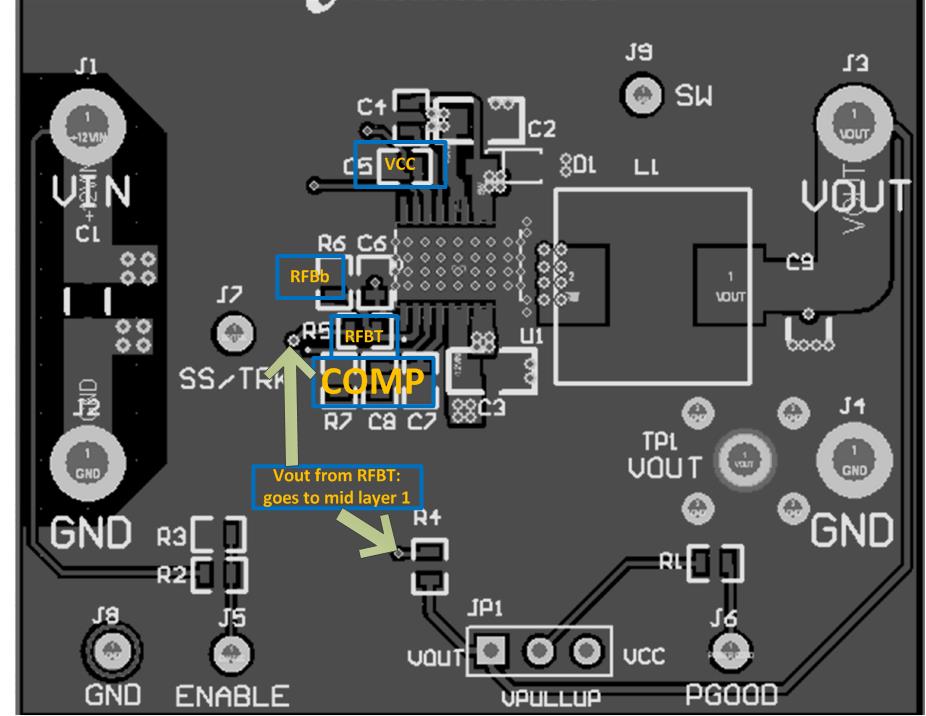
Please find attached design I did for 3.3V output and 5V output from 15V and 5V input.

I designed error feedback for correcting the voltage output in 2 options .

  1. With OP Amp .
  2. With resistor divider that get the voltage from Vesnse instead of output voltage.

The ripple is very high and when using the OP Amp is even worse.

Please advise.

Best regards,

Shlomi

DC_DC Adaptor Option3.pdf

  • Hello Shlomi,

    Thank you for sharing your schematic.

    The PCB layout for the FB trace is critical. Would you be able to share your PCB layout as well? Also, would you be able to share a waveform of SW, VIN, and VOUT with the op-amp connected and without the op-amp connected?

    One thought that I have from looking at your schematic, is that the Bottom Feedback resistor is recommended to be between 4.99kOhm - 49.9kOhm. Could you resize R5, R7, R14, and R17 to be greater than 4.99kOhm?

    Thank you,
    Katelyn Wiggenhorn
  • Hi Katelyn,

    Please find attached layout.

    Regarding waveforms I don’t have currently PCB on hand so cannot show.

    Well noted below point regrading  R5, R7, R14, and R17 to be greater than 4.99kOhm.

    Best regards,

    Shlomi

    DC_DC ADAPTOR OPTION3(LM20323) REV01.pdf

  • Hi Katelyn,

    Due to high ripple voltage output with the OP Amp I choose the 2nd option but still having relative high ripple 200-300mv.

    I found 100-200uF ceramic capacitor in parallel with the E-cap (C9 and C24 ) will improve this.

    Please advise if can recommend any other improvement?

    Do you have any comments on the layout sent to you?

    Thanks,

    Shlomi

  • Hi Shlomi,

    What load conditions are you testing where you see the large output ripple?  Can you also share the steady state waveforms of no load and loaded?

    Also, thank you for sharing your layout.  Please see my comments below:

    1. The feedback traces to the resistors must be as short as possible.  The traces are very long with the addition of the op-amp and header.  This may also be why it gets worse with the op-amp.  However, even the two resistors for the FB without the op-amp is very long.  This is very critical for the device to be able to accurately sense the FB voltage at the error amplifier.  Please see the example below.
    2. The VOUT trace from L1 should see C9 before R1.  This will allow he ground plane to increase around the IC as well.  Rpg ( R1) trace is not critical.  This can be routed through a second layer or further away from the device.
    3. The COMP components (C10, C8, R6) should be placed as close as possible to the device.  On this design, the component trace goes through the bottom layer. This would be made easier by moving R1 further from the IC. Please see example tomorrow. 
    4. AGND and GND should not be directly connected at the pins.  Have a single point ground for all device grounds located under the EP. The ground connections for the compensation, feedback, and soft-start components should be connected together then routed to the EP pin of the device. The AGND pin should connect to GND under the EP. If not properly handled poor grounding can result in degraded load regulation or erratic switching behavior.

    I have included an annotated layout of the EVM.  I annotated critical components. Please reference this image.

    Best Regards,

    Katelyn Wiggenhorn

  • Hi Shlomi,

    I am going to close this thread due to inactivity. However, if you have any additional questions on this subject, please feel free to respond.

    Best Regards,
    Katelyn