This thread has been locked.

If you have a related question, please click the "Ask a related question" button in the top right corner. The newly created question will be automatically linked to this question.

TPS63030: TPS63030

Part Number: TPS63030
Other Parts Discussed in Thread: TPS63031,

Hi,

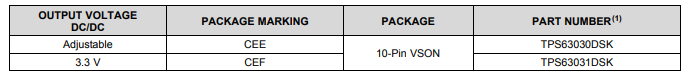
Please find the attachment below.

In the datasheet, it is mentioned that VFB is tested at two conditions of  PS/SYNC. That is "PS/SYNC = GND Referenced to 500 mV,PS/SYNC = GND Referenced to 3.3 V". Please let me Know, what is mean by GND Referenced to 500 mV and GND Referenced to 3.3 V in our circuit. Let me know, how to put PS/SYNC pin to this two conditions.

Regards

shankar

  • Hi Shankar,

    The TPS63031 is a fixed output version of the TPS63030. In the TPS63031 the FB pin is directly connected to VOUT=3.3 therefor it is written VFB is referenced to 3.3V.

    The TPS63030 is the adjustable version (Vout can be set to any voltage from its defined spec by the resistive divider) in this the VFB is refenrenced to VREF=0.5V as show in the system block diagram Figure 3.

    It is not the PS/SYNC pin that is referenced to 500mV and 3.3V

  • Hi Sabrina,
    The expected value of Vfb min value is -3% of 500mV and max value is 6% of 500mV. Output voltage min is -3% of 3.3V and max 6% of 3.3V. Please confirm.

    Thanks in Advance
  • When it is in PFM mode, yes, the VFB voltage can vary in this specified range .

    I also saw the other post on the PS/SYNC question, what is your main concern here? What are the operating conditions and end application you want to design with this device?
  • I am preparing load board for validating the buck boost converter as a internal training projects, the IC not using in any circuit.