This thread has been locked.

If you have a related question, please click the "Ask a related question" button in the top right corner. The newly created question will be automatically linked to this question.

LP3985: LP3985-2.5 output at 3.3V (no load) on two boards.

Part Number: LP3985

Hi,

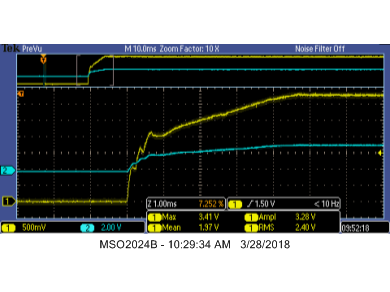
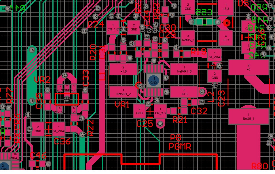
I am debugging a new design that uses the LP3985-2.5 to power a FPGA.  The same FPGA also has banks running on 3.3V.  I have a series 0 ohm resistor between the regulator and FPGA so I can disconnect the FPGA load leaving only the output capacitor.  There is 10 uF in parallel with 47 uF on the input of the LP and 10 uF on its output.  There's a 10 nF between bypass and ground.  I have two prototype boards.  Originally there appeared to be a short between 3.3V and 2.5V (under the FPGA, of course).  I removed and replaced the FPGA and the short is gone but I am using the same LP3985-2.5.  With its output now disconnected from the FPGA but still connected to its output capacitor, the LP input measures 3.359V and its output measures 3.216V.  I have a second board whose LP3985 output was originally attached to the FPGA and measured 3.3V, so i removed its zero ohm jumper.  Disconnected from its load the second board's LP3985-2.5 measures 3.24V with its input measuring 3.28.

So it is possible on the first board, the LP's output was being dragged above it's nominal 2.5V output value.  From the simplified block diagram, this wouldn't appear to damage the LP since it cannot sink current if the output is pulled above its regulation value.  On the second board, however, there is (and was never) a short, so it is difficult to explain how it is no longer regulating.  I have attached the schematic sheet.

Any thoughts are most appreciated.

Thanks,

Scott

  • Hi Scott,

    do the LPs oscillate? What happens to the output voltages of LPs when you apply a dummy load of 1...2mA?

    I think the LPs are damaged. Not necessarily from the paralleling of outputs but from dangerous differential voltages during power-up and power-down when the output voltage becomes higher than the input voltage.

    Kai
  • Hi Scott,

    From your description I would tend to agree that it is unlikely that you damaged the LP3985 by driving Vout higher than the nominal output voltage so long as Vout never exceeded Vin.  In order to help debug, could you provide a scope shot with Vin, Ven, and Vout?  It would also be good to see the layout for LP3985.

    Unfortunately E2E is a bit picky on how images are attached to posts.  Please refer to the following for the proper way to attach an image.


    Very Respectfully,

    Ryan

  • Hi Ryan,

    Thanks for the fast reply.

    Since Vin is driven by the same 3.3V source I suspect was shorted to the output, there can't be any time when Vo is above Vin.

    Here's an oscilloscope capture of in and out (enable is attached to in), a schematic of the power system and the PCB layout:

    The PCB is 6-layer with dedicated layers for +3.3 and ground.

    Thanks,

    Scott

  • Hi Scott,

    looks like the LP3985-3.3 is mounted and not the LP3985-2.5...

    Kai
  • Not true. The package marking is "LCSB" which according to the data sheet is the -2.5 part. And, I measured two of the regulator outputs while disconnected at 2.5V. Once I connected their loads, they both now measure nearly 3.3. Disconnecting their loads now they still output nearly 3.3V.

    Thanks,
    Scott
  • Hi Scott,

    I cannot see a decoupling cap close to the input pin of LP3985-2.5. C25 and C32 are too far away.

    Kai
  • Hi Kai,

    Point taken.  And you think the lack of a close input cap is causing it to output the wrong voltage or pass input to output? 

    Scott

  • Hi Scott,

    hhm, not really... But Ultra-Low-LDOs are tricky. So, it could be...

    Kai
  • Hi Scott,

    Thanks for the details and scope shot.  As  indicated the input capacitor is a bit away from the LDO which will limit its impact.  On a similar note, it is best practice to provide a same layer GND connection for external components to the GND pin of an LDO (shown in green below).  However, I do not believe either of these is causing the issue you are experiencing currently due to your scope shot.

    Could you confirm that for your second board R22 was removed before you powered up the LDO?  This is a very useful data point as it removes any potential leakage from the load biasing the output.  If R22 was not removed isolating the LDO output, would it be possible to see Vin and Vout on the same scale in a scope shot with a fresh LDO with R22 removed?  When replacing the LDO also be sure to remove any residual flux as flux can cause unintentional leakage paths.

    Very Respectfully,

    Ryan

  • Hi Ryan,

    I can't confirm that the regulator was isolated on any boards.  From here, it seems that the regulators are OK until their outputs are attached to the FPGA & other board loads.  After that, isolating their outputs shows them to be shorted (e.g. outputs at 3.3).

    I do have an additional data point.

    On board #3 (only meaningful to me), there was a 3.3V short to ground.  I used a milliohm meter to find that the short was under the FPGA.  When I removed the FPGA, the short was gone AND the 3895's output was good at 2.5V.  Upon replacing the FPGA (resoldering the same part), the 3.3V short is still gone BUT the 3895's output is now at 3.3V.  Also note that removing the isolation jumper (R22), the disconnected side of R22 (e.g. the FPGA's 2.5V supply) measures about 800 mV, which I believe to be reasonable with a little leakage through the FPGA.  Clearly there's no low-impedance connection to another signal.

    I do not have 3895 replacements, but did order a competitor's drop-in replacement.  They should arrive next week.  I am out until mid-week and will keep you updated.

    Best,

    Scott

  • Hi Scott,

    I guess that the LP3985 have been tortured so much, that you cannot expect a nominal behaviour from them. Only the heaven knows what the brave LP3985 had to endure... :-)

    I would fix the PCB problems, mount some fresh LP3985 and start from scratch.

    Kai
  • Hi Scott,

    Many loads that require multiple input rails have leakage paths internal to the load itself. This could explain why the output is biased high while the load is connected; however, it does not explain why the LP3985 is damaged when the load is removed. I do not see anything in either your schematic or your layout files that would explain the damage based with the waveforms you provided.

    Good luck with your tests with the other devices. If you would like to attempt more debugging on the LP3985, please consider ordering some sample devices from the following link:

    www.ti.com/.../samplebuy

    Very Respectfully,
    Ryan