This thread has been locked.

If you have a related question, please click the "Ask a related question" button in the top right corner. The newly created question will be automatically linked to this question.

UCC27324: Switching Speed driving 3 x CSD19506KCS

Part Number: UCC27324
Other Parts Discussed in Thread: CSD19506KCS,

Hi,

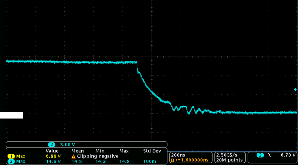
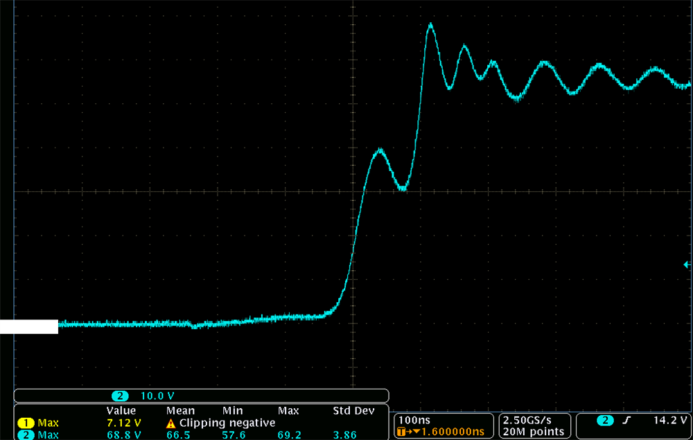
I have an application were a single UCC27324 (output channels in parallel) drives three CSD19506KCS in parallel. Each of the MOSFETs has separate 6ohm gate resistor. I want to decrease the switching loss inside the MOSFETs during turn-off. The switched current is about 85A and the switched voltage around 60V. The UCC27324 is supplied with 15V. The measured Drain-Source and Gate-Source Waveforms are attached.

Gate-Source

Drain-Source

I am thinking about decreasing the gate-resistance to increase the quite slow switching speed. Are there recommended gate-resistor values for this combination?

The datasheet of the UCC27324 states an absolute maximum current of 4.5A and minimum input resistance of 0.9 Ohm (over full range). If I decrease the gate resistors to 1 ohm I calculate an overall resistance of 0.78 Ohm (2 channels in parallel = 0.45 Ohm + 3 resistors in parallel = 0.33Ohm). Neglecting trace resistance and inductance I calculate a maximum current peak of 19A (15V / 0.78A). This is way higher than the maximum rating in the datasheet (8A for the combined channels). However the "Current Sink Test Circuit" from the UCC27324 datasheet does not have any current limiting resistance in the path between the capacity and the gate driver.

Do you think it is okay to drop the gate-resistance to 1 Ohm per MOSFET or even decrease it to 0 Ohm?


  • Hi Torben,

    Thanks for your other question on UCC27324. There are a number of ways to decrease power dissipation in your FETs when hard switching. One way is to reduce the switching transition time which requires you to reduce switching rise and fall times by decreasing gate resistor. Since each of your FETs has a 6ohm gate resistor, lowering this resistance will decrease switching transition time however it will increase the power dissipated in the driver.

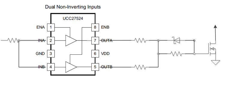
    With Qg = 120nCx3 for CSD19506KCS and a fall time of ~300ns yields a peak current of about 1A which is understandable seeing that your gate resistors are 6ohms which limit your drive current by this factor. If you want to dissipate driver power in your gate resistor then a value of 5 ohms or more is recommended.. however since you want to reduce fall times only you can simply use an anti-parallel diode on the gate resistor to facilitate a fast turn off at the expense of more noise. Decreasing this resistor too much may turn on the FET too fast leading to more ringing on the gate/switchnode. Picking a value for this turn off gate resistor if needed should be done carefully as to keep noise at an acceptable level. 

    Also for help with paralleling outputs, there is a section in the datasheet (9.2.2.2 Parallel Outputs), for matching up timing at the output stage and to prevent unwanted shoot through TI recommends, when an external gate resistor is used to add your gate resistor equally split between OUTA/OUTB to limit shoot through current. Also for ringing INA/INB should be tied as close as possible to the IC to reduce noise coupling. The inputs should slope more than 20V/us to tighten up delay matching.

    For paralleling outputs with a gate resistor and anti-parallel diode please reference the figure below. If using the diode, the external gate resistor value would essentially be split between the two resistors in the series path.

    Let me know if you have any more questions!

    Thanks,