This thread has been locked.

If you have a related question, please click the "Ask a related question" button in the top right corner. The newly created question will be automatically linked to this question.

UC3825: Problems with minimum duty cylce and Aout/Bout toggling of the UC3825

Part Number: UC3825
Other Parts Discussed in Thread: UC1825,

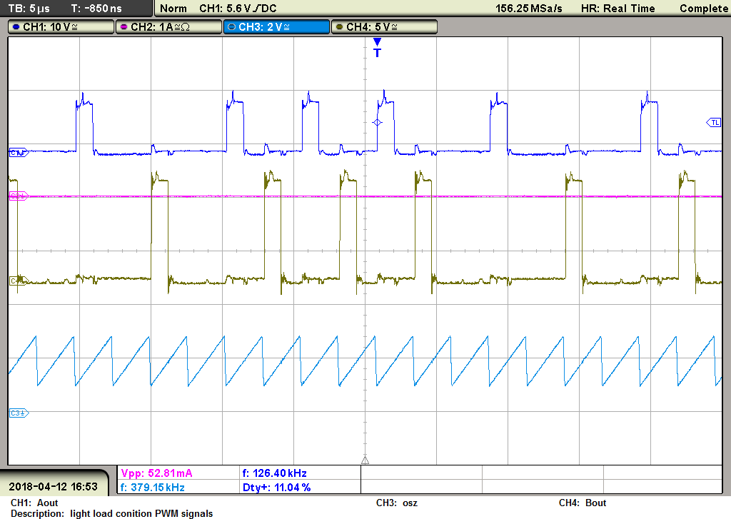
I have experienced some problems with the UC3825 when operating at low duty cycles. The device controlles a symmetrical half-bridge converter, oscillator is set to 380kHz, LEB is set to minimum (by connecting a 2k15 without any capacitor to the LEB Input). The RAMP-Input is feed with a slope compensation signal and a small amount of the transformer primary current (Peak current mode). The soft-start (pin o/c) and ILIM - function (voltag is <200mV) is not used.

The device operates as expected under medium to high load conditions where the converter operates in continous conduciton mode (duty cycle per output is arround 30%). Under light load conditions discontinous conduction mode takes place and the duty cycle is reduced. In this condition the minimum duty cylce stucks arround 20%. If lower duty cylce is needed, some pulses on the Aout or Bout output are suppressed completely. It also looks like the internal toggle-flip-flop is toggling unindentional. The effect also leads to an audible noise since the AC-voltage applied to the transformer primary is disturbed.

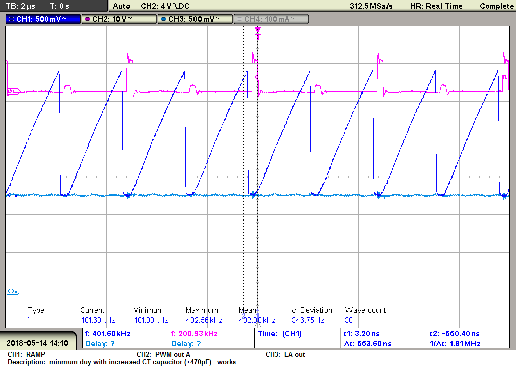
Here is a typical measurement:

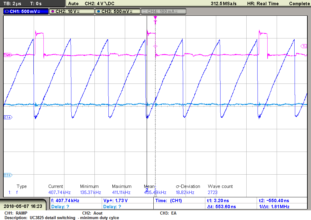
I have modified the circuit by applying pure voltage mode (as shown in the datasheet /app note) by connecting the CT and Ramp Input: The same effect but slightly lower duty cycles have been reached.

I also reduced all kind of EMC-influence by shielding and filtering of supplies and other signals -> no effect.

Lower  minimum duty cylce has been reached by reducing the source impedance of triangular signal applied to the RAMP-Input  - but the effect is still visible.

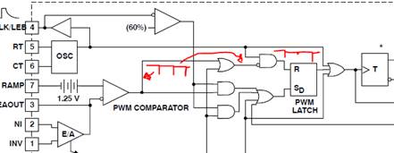
The datasheet does not give any information of minimum duty cylce (it is stated in the text that Zero duty cycle is possible); also no Information about required source impedance of the RAMP-Input.

Is this effect known? Is there a work-arround?

We currently use the UC3825 for the breadboard - but we want to use the UC1825 for the product.  Would it be the same for the UC1825?

  • Hi Franz Stoegerer,

    Thanks for your interest in this part.

    I am slightly confused by your question. You mention a LEB input on the part but the UC3825 datasheet shows no LEB input.

    The pulse width of this part is generated by comparing the E/A amplifier output with the ramp input. If you have some issue regarding minimum duty cycle I suggest that you get these two wavefroms on the scope together with the same scale. It should then be very clear why the apparent minimum duty cycle is occurring.

    Thanks

    Joe Leisten

  • Dear Joe,

    thanks for your quick response.

    For clarification: LEB means the CLK/LEB pin (pin 4 in the standard 16-pin DIL-package).

    Please finde attached a measurement of the EA pin Signal and the RAMP-Signal below. I have added 1.25V Offset between this Signal as it is in the blockdiagram.

    Note, that the ramp Signal is generated by a sawthooth-generator (therefore you will see a saw-Signal even if the PWM Outputs are Zero:

    From my point of view the RAMP Signal and the EA-Output seems quite normal - no reason to omit some pulses instead of reducing the duty cycle . There is a little noise, but this might be caused by the non-ideal connection of the ground connection of the probes.

    As you can see the Aout PWM-Output toggles - meaning that there should be a Aout every second falling edge of the RAMP saw-thooth. - I still cannot unterstand this behaviour.

    Do you have an idea?

    Best regards,

    Franz


  • Hi Franz Stoegerer,
    Thank you for the very clear information that you provided.
    I noticed that the standard UC3825 part does not have a CLK/LEB pin, but the UC3825A device does have this function. The datasheets for both devices can be found at the following links.
    www.ti.com/.../uc3825.pdf
    www.ti.com/.../uc3825a.pdf
    The UC3825A device is an enhanced version of the original part with added functionality.
    Please could you confirm for me which version of the part you are testing with, also please let me know the RT, CT and CLK component values that you are using.
    Thanks for your patience and understanding in resolving this issue.
    Joe Leisten
  • Hi Joe,

    sorry about the confusion with the A-variant.

    The following is printed on the part:

    UC3825AWD

    [Delta]U68Z22KV           (first letter looks like a "Delta")

    G4

    I have connected 540pF to the CT-pin and approx. 6.5kOhm to the RT-pin. A 2.15kOhm  is connected to the CLK-pin in order to keep LEB-time to a minimum (I also tried it without any resistor connected to CLK). - all referred to GND.

    One additonal Information: the CLK-Signal is also used for the generation of the slope compensation.(a capacitor is discharged when CLK is high). A emitter-follower is connected to the CLK-pin consisting of a 2N2222 and a 2k15 emitter resistor (input impedance of this stage should be >100kOhm)

    Best Regards,

    Franz

  • Hi Franz Stoegerer,

    I contacted Rich Valley, one of our design gurus', on your behalf. His full response is copied below:

    "Sorry for the slow reply. I hope I have something useful for you. I am really just going by the datasheet and block diagram – but I have a theory…..

     Observations:

    • Anytime an output is generated the FF it toggled. (intended only to always prevent two A or B pulses in a row and doing its job from what I can see)

    • The Toggle FF is on the cusp of not being reset for E/A levels that are above the RAMP valley – resulting in a long minimum on-time (540ns).

    The real problem, I think, is the 540ns minimum on time.

     Theory:

    Looking at the customer’s RAMP signal – he may have the discharge time too fast. The only time the logic has to reset the PWM Latch is during the portion of the discharge time when the ramp is < the E/A output. In the picture below the pulse into the R input of the PWM LATCH could be too short i.e. “swallowed” (clumsily illustrated below). This looks like what is happening.  This would explain why he is seeing the long, 540ns, minimum on-time. As E/A gets lower, the width of the reset pulse is shorter and shorter.

    I think – if he adjusts the RT/CT values to a slightly larger CT and smaller RT, then he can maintain the target frequency and get a reliable reset pulse at a lower E/A output and thus shorter minimum on-times.

      "

  • Dear Joe,

    thank your for this hint.

    Since I am out of office for the rest of this week I am going to increase the CT-capacitor as suggested on monday.

    Best regards,

    Franz Stoegerer

  • Dear Joe,

    i have increased the capacitor by adding another 470pF to the CT-pin and adjusted the switching frequency accordingly via RT.

    Now it works!

    Originally, i have selected the small capacitor to get as close as possible to the 100%-maximum duty cycle limit (in order to operate in a wide input voltage range).

    But now it is clear, that this limits the minimum duty cycle.

    I think, I can readust the CT-RT  PParameters for my application.

    Thank you very much for your support!

    Best Regards,

    Franz Stoegerer