Because of the Thanksgiving holiday in the U.S., TI E2E™ design support forum responses may be delayed from November 25 through December 2. Thank you for your patience.

This thread has been locked.

If you have a related question, please click the "Ask a related question" button in the top right corner. The newly created question will be automatically linked to this question.

REF2033: Very noisy ADC output compared to using MCU internal 3v3 refrence

Guru 54678 points
Part Number: REF2033
Other Parts Discussed in Thread: TM4C1294KCPDT,

Hello we are capturing far to many PWM pulses on output pin 5 and wonder if bypass C104 or sourcing AGND from  VIA's may lead to poor PWM noise rejection?

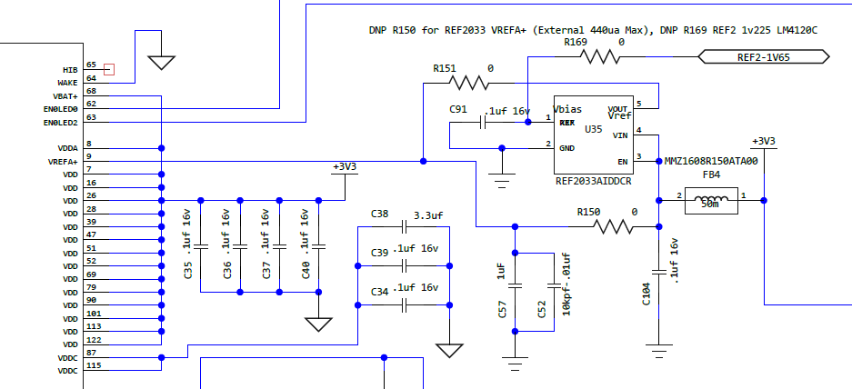
Notice C57 & C52 are required per MCU datasheet (TM4C1294KCPDT) ADC0 electrical specification for use with external +VREF. R169/150 are not populated.

The MCU internal VREF produces clean ADC samples without much if any 12.5Khz PWM spikes showing up in GUI scope widgets. What can be done to improve REF20333 circuit to stop PWM on pin 5? 

Thanks in advance for constructive ideas.

  • Hi BP101,

    There can be many reasons for PWM spikes. Do you mind showing some scope shots of the spikes as well as a shot of the reference voltage in both situations (internal vs REF2033). How are the signal captured? Probe set-up is key to getting an accurate reading.

    A short rise time combine with some parasitic L and Cs can cause the oscillations. You can try adding more output capacitance or add a series resistance ~(22-330 ohm) in the signal path for some RC filtering. 

    Also i see that you providing a 3.3V supply for voltage reference providing 3.3V. With a a slight voltage drop from the FB, the REF2033 is not within recommended conditions. I would try supplying the REF20XX with something greater, +5V to be safe.

    Hope this helps,

    Ethan

  • Hi BP,

    should Vin of REF2033 not higher than 3.3V?

    Kai
  • Datasheet 7.3 (ROC) does not make such a distinction for input voltage. Drop out is (VREF +.02 Min) and VDD is actually 3v340 and current is well blow load graph Fig 28.
  • Ethan Than said:
    You can try adding more output capacitance or add a series resistance ~(22-330 ohm) in the signal path for some RC filtering. 

    Your implying to add resistance to input pin 4 ? as we discovered ADC 440ua Max current escalates if any series resistance is added in the VREFA+ signal path.

    Ethan Than said:
    Also i see that you providing a 3.3V supply for voltage reference providing 3.3V. With a slight voltage drop from the FB, the REF2033 is not within recommended conditions

    The FB is 50mOhm but it does have 120 ohm impedance @1Mhz and we were considering a lower resistance FB in this area. It seems a real mistake was using AGND at any point. We recently switched the ADC to use DGND versus an AGND source and that helped reduce the PWM noise reduction in ADC samples.

    Seemingly the 0.1uf bypass cap placed on the input may aid AGND PWM signals flowing right into the REF2033 input.

    Ethan Than said:
    I would try supplying the REF20XX with something greater, +5V to be safe.

    And if the 2033 output ever shorts to rail the 3v3 MCU pin will get an immediate blast of 5v, that would seemingly be an unwise choice to begin with.   

  • Hi BP,

    the REF2033 needs more input voltage than VREF+10mV to regulate properly. Have a look into the datasheet: Line regulation is specified at VREF+20mV and load regulation even at VREF+0.6V. And most other parameters are specified at Vin=5V.

    You cannot run the REF2033 at Vin = VREF + "dropout voltage", because then the regulator is out of regulation. That's just the difinition of dropout voltage. Also, don't you have any noise at input and output of REF2033? This must also be taken into consideration when designing the headroom.

    Kai

  • kai klaas69 said:
    the REF2033 needs more input voltage than VREF+10mV to regulate properly.

    REF2033 regulates the input voltage very well until PWM is running for the DC inverter. checked again and the 3v3 LDO (TPS73533DRVR) is providing the REF2033 input supply 3.4v.

    The input is actually 3.4v and the line regulation is roughly 140mv over the minimum 7.3 ROC table. Graph Figure 28 starts 0ma of load and VREFA+ input maximum is only 440ua well below that.

    kai klaas69 said:
    and load regulation even at VREF+0.6V. And most other parameters are specified at Vin=5V.

    Again datasheet supply Input voltage 7.3 ROC states 5.5v maximum and the minimum VREF +0.02v per Fig 28 load graph. Dropout is 0v more relative at 1ma up and certainly not 440ua maximum load.

    kai klaas69 said:
    Also, don't you have any noise at input and output of REF2033

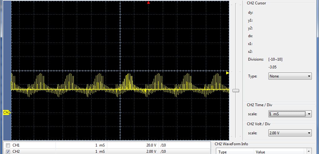
    Again that is the problem as scope capture indicates below, only when DC inverter is running the PWM dances around like Flubber the movie. Looks like wrong capacitor value on the input / output of REF2033 or C91 should not be installed if 1.65v REF is not being used?

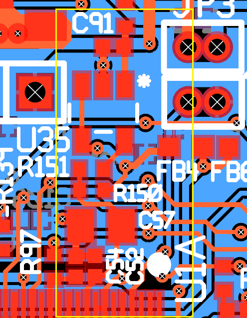
  • Below is the PCB layout (yellow box) almost identical to Figure 58.  Capacitor values being suspect in above capture peaks of 5.4v. Where DC inverter PWM frequency may range from 12.5Khz up  to 40Khz during testing. What would be the suggested values since the internal MCU reference produces much cleaner samples by more than 1/2 the noise ratio of REF2033 supplying VREFA+. We were expecting the external reference to produce much cleaner precision samples.

  • Hi BP,

    the DC inverter, what is it? A DC/DC-switcher? Or a charge pump? Where is the DC inverter drawing AC current? At input or output of REF2033? The yellow curve of scope plot, where is it measured?

    Kai
  • Hi kai,

    DC motor driver powered from 24vdc switcher. Two 680uf parallel electrolytic on DC inverter PCB yet some PWM noise there too. Above capture is on output of REF2033. A +5vdc buck switcher powers 3v3 LDO and it powers the REF2033.
  • Hi BP,

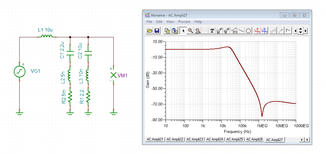
    I would try to improve the filtering at input of REF2033. Use a 10µ choke with a high resonance frequency instead of FB4. Take a 2µ2/X7R instead of C104. To dampen the series resonance of this LC-filter and to suppress the ringing put this 2µ2 cap a 10µ/X7R cap in parallel which has a 2R2/0805 resistor in series. The 10µ cap and the 2R2 resistor form a snubber, which is needed because no damping resistance in series to the 10µH choke is allowed:

    Kai

  • Perhaps the 10uh choke alone will improve input noise rejection. But what about C91, is it being useful or making matters worse since there is no load on Vbias pin 1?

    How is it that the MCU internal VREF does not have any large capacitance or inductors/snubber and there is hardly any sample noise? Might it be the REF2033 is not designed stop PWM oscillations bouncing along VIA ground plane, since it does not have a low pass filter designed into it?

    What's even more surprising is no one else on Earth has reported this issue to TI so engineers could incorporate some kind of internal low pass filtering into the REF2033 structures or post datasheet warnings. I always seem to be the first one who says "Hey what's going on here."
  • Hi BP,

    I know what you mean... :-)

    Well, I have made the experience that using a solid ground plane and almost parnoid looking filtering of every input and output is sometimes the only way to make a circuit properly work.

    And there's a huge difference between a voltage reference and a voltage regulator. A voltage regulator must withstand all sorts of load currents and input ripples. A voltage reference, on the other hand, is often overstrained by even the least input ripple or dynamic load current.

    Kai