This thread has been locked.

If you have a related question, please click the "Ask a related question" button in the top right corner. The newly created question will be automatically linked to this question.

TPS7A54-Q1: Unstable V_NR/SS Voltage After Changing C_NR/SS Cap Value

Part Number: TPS7A54-Q1
Other Parts Discussed in Thread: CDCI6214,

Hi,

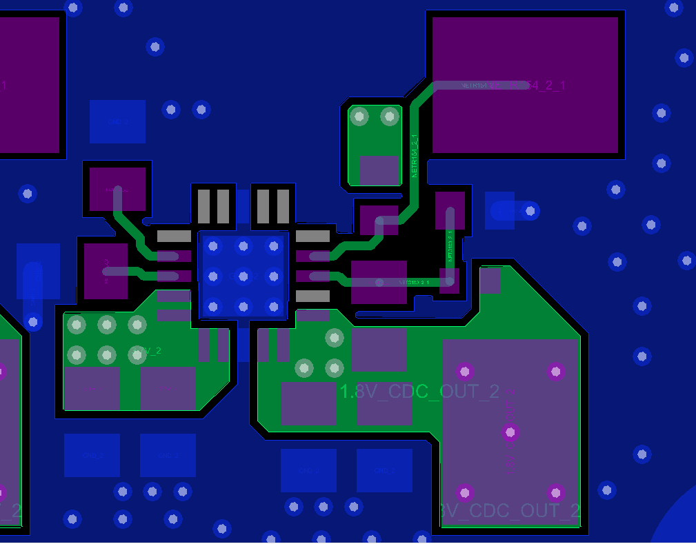
Our team recently created a board where we need to supply power to a CDCI6214, and this device requires a voltage supply ramp time faster than 3 ms. We have chosen to use the TPS7A54-Q1 to provide 1.8V to the device, but used a 100 nF cap on the NR/SS pin. This created a voltage supply ramp of around 10-12 ms, which has created issues for us due to the CDCI6214 power supply ramp time requirement. Please find the TPS7A54-Q1 schematic and layout below.

Schematic:

Layout:

Before reworking the board, I was able to see that the NR/SS pin voltage was a stable 0.78V, and VOUT = 1.778V, as expected.

However, after I changed this cap to 10 nF per datasheet recommendations, the NR/SS pin voltage became 0.2-0.3V, and over time, the NR/SS voltage slow reduces, almost like it is discharging somehow. The Power Good voltage is 0.2V and VOUT < 1 V.

Next, I removed the cap completely from the NR/SS pin. When I did this,the NR/SS pin voltage started off at 1.2V, and over time, the NR/SS voltage slow reduces as well. However, this time, the Power Good voltage and VOUT appear to track linearly with a voltage approximately equal to VIN.

I am not sure if this is an indication of a damaged IC or if this is expected behavior when changing the cap value. Any advice about what is going on?

Thanks,

Michael

  • Hi Michael,

    The NR/SS pin provides access to the internal reference so that an external capacitor can help filter the reference. From your description, it sounds like you may have an unintentional leakage path on the NR/SS pin (such as residual flux from your rework). As the output voltage is a gained up version of the reference voltage, if Vref is being pulled low, then Vout will be low as well.

    Since the issue began during rework at the NR/SS pin, can you do a visual inspection to ensure that all residual flux has been properly cleaned?

    Very Respectfully,
    Ryan
  • Hi Ryan,

    Thanks for the quick response!

    Based on the datasheet formula to derive VOUT based on the voltage observed at the NR/SS pin, the math checks out and I see that the NR/SS pin voltage allows me to calculate VOUT reliably, even if the NR/SS voltage is not the 0.8V I expect. This may suggest the TPS7A54-Q1 is still functioning correctly.

    I will check on the residual flux to make sure it is properly cleaned. This issue has only ever happened to me following rework, so I think the cause is linked to the rework somehow. When we receive boards back from the fab, the supply voltage has always been reliable coming out of these regulators otherwise.

    Assuming rework is the issue, would this leakage path also explain why the NR/SS voltage starts off well above 0.8V when no cap is populated on the NR/SS pin? I can understand the discharge behavior coming from an unintentional leakage path, but my intuition would assume that the NR/SS voltage start off at 0.8V and discharges through a leakage path rather than start off well above 0.8V. Any ideas there?

    Thanks,

    Michael
  • Hi Michael,

    When the LDO is disabled, the reference is also disabled.  After the LDO is enabled, Vref will ramp.  Keep in mind that Inr/ss is less than 10 uA; therefore, it will only take a small amount of leakage current to influence Vref.  

    If the small leakage path came from flux during rework, this would effectively look like a resistor between NR/SS and GND.  This resistor would be there regardless of if you have a Cnr/ss populated or not.

    Another thing to consider is that when you measure the reference voltage at NR/SS, your equipment could also be adding a load and influence the reference voltage.

    Very Respectfully,

    Ryan

  • Hi Ryan,

    After some more debug the past few days, I believe the issue is due to residual flux trapped underneath the TPS7A54-Q1, as you suspected. I think it is due to flux under the device because, after cleaning the surface and around the pins with isopropyl alcohol, I still notice this strange discharge effect.

    I have also noticed that, even though the NR/SS voltage measures much higher than expected (anywhere from 1-2V), if I wait for 5-10 minutes, the voltage on the NR/SS pin eventually settles back to around 0.8V and remains steady as long as I continue supplying VIN. I wonder if there are two types of leakage paths caused by the rework, one going to GND and another going to VIN to form a voltage divider initially on power up:


    Once the NR/SS voltage settles around 0.8V after 5-10 minutes, I am finally able to see the correct programmed voltage on the LDO regulator output and it holds steady. It seems that eventually the leakage path "disappears" after a period of "on time."

    As an additional debug measure, I had some boards exhibiting this issue reworked with a new IC. During the process, the footprint on the board is thoroughly cleaned before mounting the new IC on. For these boards with new ICs, I had no issue seeing the correct voltage output immediately on power up. No discharge effect observed there.

    In my application, it is most important that the LDO provides a supply much faster than 3 ms. To do this, I have decided to remove the cap on the NR/SS pin. I see on the datasheet that this means I will not get maximum AC performance. but aside from that, are there any other obvious "penalties" I pay in exchange for the fastest possible rise time coming out of this LDO?

    Thanks,

    Michael 

  • Hi Michael,

    An external Cnr/ss serves two functions. The SS function is the softstart. A larger capacitor will increase the startup time and a smaller (or no capacitor) will decrease the startup time.

    The NR function is when the LDO is fully enabled. Here the capacitor performs a filtering function on our internal reference. Decreasing or eliminating the capacitor will increase the LDO noise as depicted in Figure 14 of the datasheet.

    Very Respectfully,
    Ryan
  • Hi Ryan,

    I think the LDO noise trade-off incurred by removing the C_NR/SS cap is acceptable in my current use case. 

    This resolves my questions. Thanks again!

    Regards,

    Michael