Other Parts Discussed in Thread: TINA-TI,
Tool/software: TINA-TI or Spice Models
Hello,
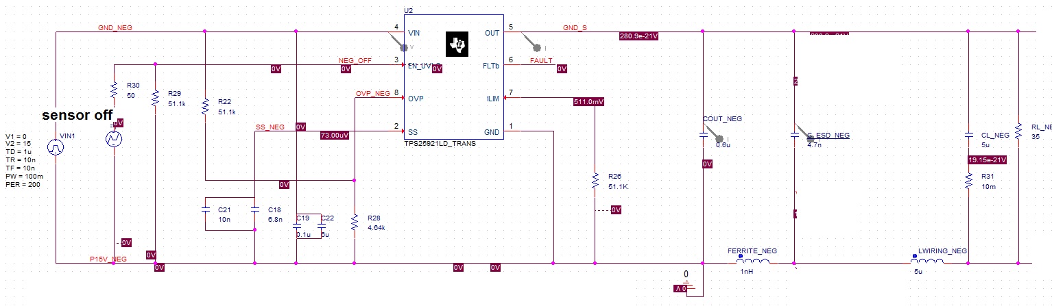
I am simulating the TPS25921L to protect a -15V, 500mA power supply (OUT pin connected at the PCB ground and GND pin connected to -15V output). I added a few parasitic elements like wiring inductance, load resistance/capacitance at the VOUT pin.
I see some inconsistencies in the device behavior during this simulation
1) VOUT voltage follows the SS pin voltage ( VOUT = Gain x Vss as per datasheet?)
When the pspice ground is moved to TPS25921 GND pin, the ramp up is correct, but during switch off, there a large current spik flowing in the VOUT --> VIN path, even when VIN voltage > VOUT.
Is this a issue with the simulation model or expected device behavior? In my view, a series diode at the VOUT pin should suffice to block this.
Thanks and regards,
Anurag M