This thread has been locked.

If you have a related question, please click the "Ask a related question" button in the top right corner. The newly created question will be automatically linked to this question.

TPS62821: tps62821 EMI Reduction Optimization

Part Number: TPS62821

Dear E2E:

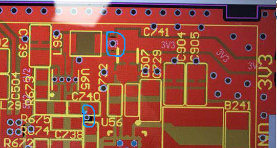
Compared to the schematic and pcb layout, i found the via near L99 in wrong position, i should be behind the output cap C741.
The input cap C739 was not very perfecter.

I check the sw waveform, it's bad.  The output point waveform through Spectrum Analyzer is not very good too.
I have no idea how to improved the performance, now i add a ferrite bead in sw point.

may i know your suggest ,thanks 

SW Waveform:

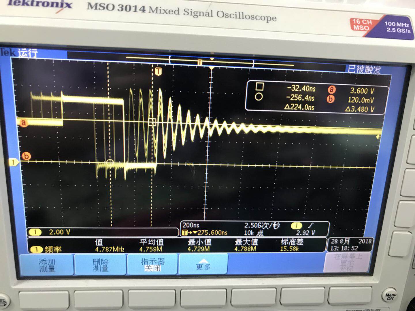
Spectrum Analyzer Waveform:

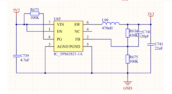
Customer schematic :

PCB Layout:

  • Hello dear User,

    your waveform does not look bat, actually. Depending on the load condition, the device will work in DCM to enable PSM. And your waveform is just a typical DCM one. What is the load current ?

    Is the spectrum analyzer directly connected to the output capacitor? How is the input impeadance setup on the analyzer? If you have the option, you should set it up to 1 Meg.

    Why do you think your spectrum is bad ? what are you comparing it to? Do you have a mask specification to fulfil ?

    The layout can also be inpmrove:

    -what is the via circled in blue for? Doe is create aburied 3.3V power plane? If yes, you already know you should put it to the right of C741
    -the input capacitor C739 is the most important passive to be placed. It should have the shortest path to GND and VIN pin as possible, and in your case it can be improved. Never do this connections through vias, they must be direct as shown in the layout suggestion on the DS at page 21.
    -if you have really though spectrum masks specs, you can place an additional Cin and Cout of a small value, but which impedance behaves as a capacitor at higher frequencies (GRM022R71A471MA01 is an example for X7R requirements)